Any particulars I have to follow when using a Mini54 for the first time?

Status
Not open for further replies.

Constantin

Well-known member
So I decided to have some fun and try out making a Teensy 3 board using the Mini54 option. However, I am encountering a very unhappy chip - though I have power in all the right places and no shorts, the board behaves as if it was not plugged in. I have no doubt that the fault is mine, I am simply trying to track down a reason.

I get 50 retries to no avail, so I wonder whether I cooked the Mini54 somehow or the Kinetic chip. Is there a way to see if the Mini54 or the Kinetic are 'alive', i.e. some sort of heartbeat program / protocol? Unfortunately, I do not have a LED on SCK, but if the Mini makes the Kinetic blink the way I remember the Teensy 3 does on arrival, I could look for that with my logic analyzer or oscilloscope.

I'll post the connections I made next. There seems to be no difference between the real world vs. the planned connections - I used my DMM to determine the resistances and if there were any shorts to other pins. I found none. However, the very large lands around the Mini54 as designed in Eagle made for a big mess and I had to remove a lot of excess solder (i.e. thick dollops of flux and braid necessary). I wonder if I managed to "cook" the mini54 in the process.

In other interesting news, I'm pretty certain that OSRAM has their PointLED cathodes and anodes reversed in the spec sheet. They only emit light when hooked up in 'reverse'!

state = 0
get_line: "code_size:131072"
get_line: "EOT"
status read, retry 21
send: status - at Sun Nov 10 10:43:58 2013
sent: status - at Sun Nov 10 10:43:58 2013
get_line: "dir:/var/folders/10/k4zcgfcd7rg_wnk00_snp3sr0000gn/T/build3843299479181835897.tmp/"
get_line: "file:Blink.cpp.hex"
get_line: "readable:1"
readable = 1
get_line: "auto:1"
auto = 1
get_line: "online:0"
online = 0
get_line: "online_count:0"
online_count = 0
get_line: "offline_count:0"
offline_count = 0
get_line: "state:0"
state = 0
get_line: "code_size:131072"
get_line: "EOT"
status read, retry 22
send: status - at Sun Nov 10 10:43:58 2013
sent: status - at Sun Nov 10 10:43:58 2013
get_line: "dir:/var/folders/10/k4zcgfcd7rg_wnk00_snp3sr0000gn/T/build3843299479181835897.tmp/"
get_line: "file:Blink.cpp.hex"
get_line: "readable:1"
readable = 1
get_line: "auto:1"
auto = 1
get_line: "online:0"
online = 0
get_line: "online_count:0"
online_count = 0
get_line: "offline_count:0"
offline_count = 0
get_line: "state:0"
state = 0
get_line: "code_size:131072"
get_line: "EOT"
status read, retry 23

.
.
.
.

status read, retry 48
send: status - at Sun Nov 10 10:44:01 2013
sent: status - at Sun Nov 10 10:44:01 2013
get_line: "dir:/var/folders/10/k4zcgfcd7rg_wnk00_snp3sr0000gn/T/build3843299479181835897.tmp/"
get_line: "file:Blink.cpp.hex"
get_line: "readable:1"
readable = 1
get_line: "auto:1"
auto = 1
get_line: "online:0"
online = 0
get_line: "online_count:0"
online_count = 0
get_line: "offline_count:0"
offline_count = 0
get_line: "state:0"
state = 0
get_line: "code_size:131072"
get_line: "EOT"
status read, retry 49
Please press the RESET BUTTON on your Teensy to upload your sketch. Auto-reboot only works if the Teensy is running a previous sketch.
 
Last edited:
The Mini54 resides on a daughterboard because that was the easiest way for me accommodate the two chips on a 2-layer board.

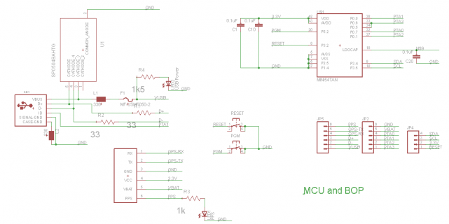
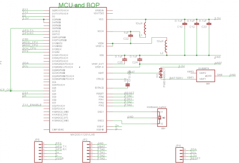
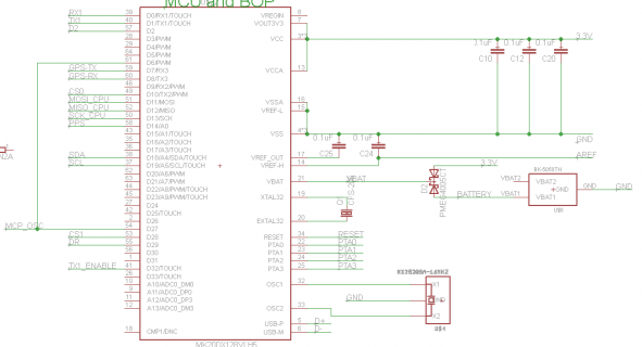
Here are their circuits. Did I miss anything obvious?

First, the daughterboard - it features a TVS array in addition to the usual suspects found on the Teensy 3 board.
Daughterboard Circuit.png

The main board interfaces with the daughterboard via 3 single-row headers. I confirmed that the two connection lists match up.
MCU.png
 
Last edited:
Two things come to mind from the schematic:

1 - it looks like you've got VOUT33 on the MK20 disconnected but on the PJRC schematic it's connected to VCC/VDD. I did a quick glance through the MK20 datasheet and it says you can leave it floating if you don't use USB at all, but section 3.9.1.2.2 makes me think the connection should be there…

2 - Have you checked the mapping of the USB connector symbol to the pads? On the schematic you've got (top to bottom) +5V, USB+, USB-, ID, GND, but actual wiring is +5V, USB-, USB+, ID, GND (USB + and - reversed).

Other random thoughts:

It looks like you're using a different library part than I am; I've used this one http://forum.pjrc.com/threads/24006-Eagle-library-for-MK20DX128VLH5?p=34199&viewfull=1#post34199 for the mk20 and mini54 and it mostly works. I'm sure you've checked the pinout but if you want to post it I'll have a look.

In my design I didn't connect the USB ID pin because my connectors don't have it. I don't think it will affect anything; I think it's only needed for the USB On The Go, but you could try cutting the trace just in case…

I don't have anything like the SP0504BAHTG in my design; I just go straight from the USB data pins to the series resistor into the MK20. I don't think it would cause any problems but again, you can try removing it to try to isolate the issue.

Regarding cooking the Mini54 - this is a possibility. I have one prototype where I had to clean up some bridges as well, and the circuit works but only after reset. On power up it just sits there and does nothing no matter how long I wait; as soon as I press reset or upload new code (and press the program button) all runs as expected. An earlier prototype with the same MCU layout came out of the oven with no bridges, so no rework necessary, runs perfectly.

[edit - typos]
 
Last edited:
Is there a way to see if the Mini54 or the Kinetic are 'alive',

A quick check for the Mini54 involves watching the RESET and PROG voltage while you press the button. Both should be 3.3V initially, because the Mini54 implements weak pullup resistors on both pins. If they're not 3.3V, the Mini54 is either dead or stuck trying to do something with the Kinetis chip.

However, a completely blank Kinetis chip will be continually watchdog resetting itself. So you'll observe a small DC voltage on reset, because Kinetis pulls its own reset signal low. With a scope, you'll see that small DC voltage is actually a waveform that's usually low but goes high briefly. If you're getting that, the Kinetis chip is probably alive, but hasn't ever been programmed. Disconnect it from the Mini54, so you can do this next test.

While the Mini54 is pulling both RESET and PROG high, and RESET isn't being pulled low repetitively by the Kinetis chip, press and hold the button. Obviously PROG will go low, since the button shorts it to ground. If the Mini54 is working, it will pull RESET low when it sees PROG go low. If RESET doesn't go low in response to PROG going low, then the Mini54 is dead.

These simple tests probably won't give you much insight as to what's wrong with your system, but you can at least get some indication of the 2 chips are still alive and functioning.


Also, VOUT33 must have 3.3V, either from the on-chip regulator or from 3.3V applied externally, for the USB to work, because the USB transceiver inside the chip is powered from that pin.
 
1 - it looks like you've got VOUT33 on the MK20 disconnected but on the PJRC schematic it's connected to VCC/VDD. I did a quick glance through the MK20 datasheet and it says you can leave it floating if you don't use USB at all, but section 3.9.1.2.2 makes me think the connection should be there…

Excellent observation. I was under the impression that one would ideally not backfeed a voltage regulator, even if nothing is attached upstream (i.e. VREGIN). I have since retrofitted a single wire that runs from 3.3V to the output of the regulator. So far, with no effect. I also replaced all the OSRAM PointLEDs and attached them with their 'Cathode' on the positive side of things and now they work. (Just not as initially expected)

2 - Have you checked the mapping of the USB connector symbol to the pads? On the schematic you've got (top to bottom) +5V, USB+, USB-, ID, GND, but actual wiring is +5V, USB-, USB+, ID, GND (USB + and - reversed).

I will look into that again, but for now, a review of the pinout IRL suggests that D- is D- and D+ is D+. I will double check to confirm D+/D- assignment by DMM with a USB-A cable.

Yes, the MK chip came from my own library and chances are I will also author a Mini54. The long pads that may make drag soldering easier threw me for a loop with my paste/reflow oven approach. The pinout for the Teensy chip is below and I appreciate your willingness to have a look at my pin assignments!

pins.png

I may also drop the ID pin or GND it, as most USB-A/Micro-B appear to anyway. I will attempt to isolate the problem as per your and Paul's suggestions. My money for the time being is on a cooked Mini54 chip. But the logic analyzer will confirm all that tomorrow, I hope!
 
Last edited:
I didn't have enough time to check out all the IO pins on the left side of your MK20 but everything on the right looks correct to me.
 
I didn't have enough time to check out all the IO pins on the left side of your MK20 but everything on the right looks correct to me.
Hey I really appreciate that!

What's also interesting is having a go with the Eagle library for the Mini54 and adding a standard TQFP-48 variant to the custom footprints enclosed. For one, the pads are thicker and shorter on a standard TQFP-48. However, they are also inset more, such that traces I have put down based on the current footprint design would interfere when used with a standard TQFP-48 footprint. My guess is that it comes down to the current Mini54 footprint being aimed at smart-board-like enthusiasts, while the standard TQFP-48 design is aimed at reflow soldering.

That is, the Mini54 pad layout I downloaded from this site seems to have little area under the pin to form a "heel". I will try a standard TQFP-48 layout instead. It will require me to make minor adjustments to the circuits but not a big deal. I was very happy with how nicely my Kinetis came out, not a single bridge, and very clean, despite a similar pitch and even more pins.
 
As a follow-up, it appears to be a fried Mini54 that prevented the first board from working. Today, I made another daughterboard with a second Mini54 and both MK20's are working happily away blinking lights and so on.

I will attempt to see if the TVS diode is perhaps at fault first, but I really doubt it (i.e. remove it just in case)… Then, I will attempt to drag-solder a new replacement Mini54 using leaded solder instead of the Pb-free stuff I usually use to keep the temperatures down.

Thank you again for the systematic approach to determining where the issues may lie, Paul. Also big thanks to potatotron for the circuit review. As I mentioned above, the current Mini54 pads are not in the right places to provide a nice heel on the backside of the pins. I will happily submit a new footprint variant once I confirm it works.
 
As I mentioned above, the current Mini54 pads are not in the right places to provide a nice heel on the backside of the pins. I will happily submit a new footprint variant once I confirm it works.

I'd appreciate that. I'm actually going to reflow another prototype today, and you're right the existing mini54 footprint isn't the easiest to use for that.

Glad you got your circuit working.
 
Glad you got your circuit working.

Hey, if it wasn't for an excellent community here, this manufacturing engineer would still be stuck at square one. Instead, I have a shoe-box full of useless PCBs to use as frisbees! :p

Anyhow, used some chip quick to lift the old Mini51 today and some careful soldering to get the replacement onto the board. This daughterboard now works beautifully. I am not sure how quickly I will order my next set of PCBs because I'm currently experimenting with everything here software-wise to make sure it's happy before I put in another hardware revision. There are a lot of features to check on, from 1-wire sensors to power measurements.

Thus, would you prefer I upload the new Mini51 footprint as an untested reflow profile? I got the outline from a reputable library (ADI) and the chip dimensions, pad sizes, etc. seem to line up nicely. If you'd like to have a look, I'll be happy to post it here.

I fixed mine the same way -- reworked the traces with a soldering iron and patience.

It sounds like your design is similar to mine -- I also have the MK20 and most components on one PCB and the Mini54 + USB port + expansion headers on a 2nd PCB.

My current Mini54 board is now working but the physical layout has problems -- the USB receptacle and the power plug are too close together and (due to a stupid basic math problem on my part) one row of headers is 0.05" misaligned.

So, I need to do another rev of the Mini54 board. If you wouldn't mind sharing the library I'll be happy to test it out with my next rev, and if it works we can have Paul S post it for everyone else.

Thanks,

Chris
 
So, I need to do another rev of the Mini54 board. If you wouldn't mind sharing the library I'll be happy to test it out with my next rev, and if it works we can have Paul S post it for everyone else.

Hi Chris, I'd be happy to upload the zipped lbr. It should be attached.

Have a look, but my review suggests that the pads are I would expect them to be and the wider pads combined with a greater inset should help with securing the bootloader chip properly to the board in a reflow setting. Some of your signal lines underneath the chip may have to move slightly to accommodate the new pad locations.

Please also review the pins, etc. just to be sure, it looked OK to me and when I replaced one chip with another, none of the signals seemed to migrate to different pins. But I don't want to cause any more pain, like for the gentleman on the first generation Teensy 3 library that featured pinholes that weren't wide enough for common headers. :(

My next daughterboard also features revisions, such as a 12mm coin cell holder to keep the VBAT energized on a header I have there for a Fastrax UP501 GPS receiver. Should allow that device to start up faster. Also eliminated the USB-ID line on the Mini-B connector and GND'd it. I also deleted the reset button I used to have on-board, completely useless as far as I can tell. Now the board only features a PGM button. :D

EDIT: NEW LIBRARY HERE:
 

Attachments

  • Teensy_DIY_v1.0.zip
    11.2 KB · Views: 89
Last edited:
Thanks. I've started revising the schematic & layout for my next prototype version; I'll use your Mini54 part & verify etc.

I'd like to have the changes done and boards ordered next week and hopefully built before Christmas. I'll report back.
 
Status
Not open for further replies.
Back
Top