Using External AREF with ADC

Status
Not open for further replies.

cocis

Member
Hi all,

I am very new to MCU and electronics and this this is my first post in this forum so I apologise in advance if this may seem a very basic question.

I am developing a Teensy 3.1 solution to use a Toroidal CT whereby I need to measure Frequency, Current and Voltage from the external system.

The frequencies I need to measure are all in the audio spectrum 20Hz - 20KHz (approx)

I push the signal from the current CT into my Digital signal processing electronics whereby a Schmitt trigger provides the nice waveform from the ugliest of input waveforms thereby allowing the MCU to successfully monitor the frequency.

My issue is over measuring the Current as this will range from 1mV to 500mv where 500mV = 5A.

If i understand things correctly I really need to bring the 500mV signal to the max of the AREF of the ADC.
I could use a trimmer to on the AREF to compensate for PSU fluctuations, or use the Internal ref which i believe is 1.195V on the Teensy 3.1.
The preferable option i believe is to use an external voltage reference chip which cannot be more than the Teensy 3.1 power supply according to the post. https://www.pjrc.com/teensy/adc.html


I would like to make the AREF as large as possible and use an op amp to offer the signal at its max level. I will also use a precision full wave rectifier op amp to offer the signal as a positive signal only to avoid the need for a rail to rail supply op amp and allow me to perform an RMS sample.

I have a couple of questions
1) What is the largest value for a precision voltage chip i can use to apply to AREF? Assume i am powering the Vin on the Teensy with a 5V regulator.
2) Can I simply connect the output from this voltage reference directly to the AREF or do i need to cut any PCB pads first. (I cant find a simple diagram that shows me how to do this)
3) Could I use a low AREF and use a MCU controlled (SPI) variable gain op amp (or digital pot) to offer all signals to the ADC at a higher level (maybe important for the 1mv signal) and then scale back by the gain applied.
4) Am I over complicating this task. I "simply" need the best accuracy possible.

Any advice or guidance from the experts would be gratefully appreciated.

thank you and apologies for my noob questions.
 
Last edited:
It might be easier to use an RMS-DC converter IC like one of these:
http://www.analog.com/en/special-li...ters/products/index.html#RMS-to-DC_Converters


Thank you very much for the quick response.

I have read through the literature and I think this chip would do the trick although it does scare me as it is a surface mount and appears to be relatively expensive and i have never used one before.

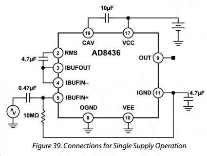
If I understand it right I just feed the CT output straight into the AD8436A (on pin 5) and put the output (on pin 9) into the Teensy 3.1 ADC as per the attached schematic taken from the datasheet?

The CT has a burden resistor R across its terminals and therefore will deliver the Voltage change into pin 5 and I will get the RMS voltage out on pin 9.

I then simply need to scale the RMS by a factor W that defines the winding ratio from primary to secondary to get the RMS Voltage in the main cable.

I assume I can then simply calculate the Current RMS through ohms law (i.e. V-RMS/R = I-RMS)

Is this understanding correct?

I also assume if the CT produces a range of 1mV to 500mV then i should perhaps put this through an op amp before passing it to the AD8436 to ensure the maximum output on pin 9 equals my AREF value on the Teensy 3.1.

Therefore AREF * SQRT(2), i.e. for 3.3V AREF = 4.667V so a maximum gain of 9 on the op amp as 500mV * 9 = 4.5V.

The flow through the sausage machine would therefore be:
CT AC Signal 500mV ------> Op Amp (Gain 9) = 4.5V -------> AD8436 -----> RMS = 4.5V/SQRT(2) = 3.3V Approx (not sinusoidal) -----> Teensy ADC ----> Divide by 9 to remove gain.

Apologies if I am confusing myself or anyone reading this.
 

Attachments

  • SinglesupplySchematic.jpg
    SinglesupplySchematic.jpg
    96 KB · Views: 438
Last edited:
1) What is the largest value for a precision voltage chip i can use to apply to AREF? Assume i am powering the Vin on the Teensy with a 5V regulator

you've probably seen the relevant AREF threads -- anyways, fwiw: my understanding is:

- it can't be larger than VDDA, which is 3v3.
- you need to use a shunt type reference such as lm4040. or else, you have to remove the 470R resistor that connects VREFH to VDDA.
- when using said lm4040s, 3v0 is the largest value you can use (also they don't come in 3v3) (i only ever tried 2v5; the datasheet for a 3v0 version says minimum current is ~ 60 µA, so that should be fine (Vs = 3.3v, Vr = 3.0v. so (Vs-Vr)/470R = 0.63mA)).
 
Thank you very much mxxx

That certainly clarifies many of my initial questions.

With a maximum current limit of 15mA for the LM4040 2.5V version this therefore yields (5 - 2.5)/470 = 1.7mA i.e. > 60µA & < 15mA so I should be fine.

Does this mean I can connect the LM4040 2.5v directly between AREF and GND pin then simply use analogReference(EXTERNAL) in the setup?

If I do this will I be fine without removing the Vin-Vusb providing I turn of the external power supply before connecting the USB to program the Teensy?

I'll post an image of what I am trying to achieve overall shortly for clarification.
 
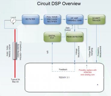
Here is an overview of the circuit components that I am thinking of using which should graphically explain my first post.

circuitOverview.jpg

As an afterthought , I'm not convinced my strategy of boosting the signal is correct, perhaps I should be looking at scaling down the AREF on the Teensy instead to achieve better resolution based on the signal peak level.
Is there a chip out there that can achieve a variable precision reference or should this be a set of MCU switched transistors to AREF with various value precision voltage references behind them?
 
Last edited:
Does this mean I can connect the LM4040 2.5v directly between AREF and GND pin then simply use analogReference(EXTERNAL) in the setup?

If I do this will I be fine without removing the Vin-Vusb providing I turn of the external power supply before connecting the USB to program the Teensy?

yep, you just connect it to the AREF and AGND pins.

as to cutting Vusb -- that's a different matter really, the 3v3 come from the onboard regulator in either case.
 
Thanks mxx.

I think i may have blown my LM4040 precision reference as it doesn,t seem to give me the required 2.5V.

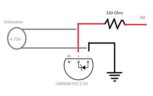
I have the TO-92 package and connected -'ve to ground and added a 5V supply to the positive pin via a 330 Ohm resistor. 5-2.5/330 = 7.57mA so should be ok.

When I measure the voltage on pin 2 to GND, I get 4.72V and not the expected 2.5V. Thought I would test this before connecting it to the Teensy and pretty pleased I did.

Is this FUBAR or am I doing something wrong?

LM4040.jpg
 
check out the schematic, that should make things obvious:

https://www.pjrc.com/teensy/schematic.html

the 470R is already on the teensy and tied to 3v3. so literally, all you need to do is to connect the two pins to AGND and AREF. 5V isn't involved, no external resistors either.

if you want to supply it externally, you have to remove the 470R resistor (though there's examples of people managing without removing it).

http://forum.pjrc.com/threads/26330-Where-is-the-470-Ohm-Resistor-on-Teensy-3-1
 
Thanks for the great links.

Sorry mxxx I may have misled with my previous post. This was my attempt to drive it on a breadboard in isolation to check if it is working.
 
ah, ok. well, i'm no expert on diodes (or anything (even remotely)), but maybe it'll need some load to work -- try with a 10k or resistor across cathode and ground?
 
No worries, neither am I. I have ordered 2 more LM4040 to test in isolation (same manner) before I connect between AREF and ground Hopefully by documenting my own mistakes others will avoid them.
Great forum, great people.
 
Thank you mxxx, and to answer you question "No I haven't" but now I will. If you say its worth trying then that's good enough for me :)

My simple mind based on the data sheet thinks Rs = (Vs-Vr)/(Il+Iq) <Ref: last line of page 25 from the data sheet http://www.adafruit.com/datasheets/lm4040-n.pdf>

In my case (post #8) I theoretically think Il = 0: Therefore (Vs-Vr)/Iq

Which results in (5V-2.5V)/(Iq ) where Iq = Current flowing diode only as Il=0

Current flowing through diode should be > 65µA and < 15mA for the LM4040 to work

I will try this tomorrow and post my results for no load and a 10K load between the +'ve central pin and GND.

Once again thank you mxxx for suggestions of things to try.
If it works, or reveals the issue or a clue to resolution, I owe you a pint my friend :)
If it doesn't, I owe you two pints for trying :)
 
Last edited:
no worries, i'm just guessing it might have to do with the (very highish) impedance of your voltmeter. the circuit i posted is advertised is something to test your multimeters with, so ..

at any rate, using a lm4040-2.5 in between AREF and AGND works just fine, so it's probably overcomplicating things when you breadboard it in isolation.
 
Yes, I believe this will work.

Since you are only interested in the AC component of the CT's output, you could connect the CT to the RMS pin directly via a capacitor (4.7 uF as shown) -- you don't need to connect to IBUFxxx.

Be aware that the input impedance is about 18 kΩ which is in parallel with the 200 Ω burden; thus making a small (1 % ) gain error.

The other ICs (e.g. AD636 which is available in a DIP package) could also work -- if you power it directly from the 5 V supply.

The AD8436 has very low input offsets and errors -- you don't really need to use an additional opamp. If you did, the IBUF could be used.
 
Thanks JP I had a look at the AD636 and it seems very expensive > £14 GBP

I have ordered 2 x AD8436 (circa £4 GBP) and some surface mount breakout boards and will give it a try when they arrive.
 
mxxx I tested the Voltage reference and have what appears to be an open circuit between the LM4040 and ground (#7)

I have 4.72V (sorry not 5v as previously stated) in and 4,72V after the 330 Ohm resistor so no drop which would be expected on a complete circuit if the zener was open.

I would have expected the ref diode to drop 2.22V (given the 4.72V potential against it to open the gate) and therefore see 2.5V on the output when measured in accordance with (#7)

Am i right in concluding that this component is fried or is my interpretation of electronics fundamentally flawed :)

On a positive note I have 2 more LM4040 to try tomorrow so I may either reach my own conclusion or commit further components to the fryer and be none the wiser :)
 
I am doing similar measurements but I avoided the use of the ADC inside the Teensy as too cumbersome/limited to work with for a bipolar signal.

I have had very good luck with the MCP3910 series of analog front ends from Microchip that live for this sort of assignment. There is a steep learning curve in getting them set up, get good readings, and so on but between the bipolar input (perfect for your range, BTW), the PGA, true 16-bit resolution, and sampling rates in the thousands/s, I couldn't ask for much more. In my (very limited!) experience, the cost of a proper Op-amp setup (or two) for the front end of the Teensy (to feature low impedance, etc.) is more expensive and difficult to implement than a MCP3910 that can talk directly to CT coils, rogowski coils, transformers, etc.

If your measurement needs are more basic, I suggest investigating a floating input like the ones used by the open energy monitor folk on the Arduino. No op-amp needed, relatively simple to implement, and inexpensive. Plus, you have libraries at your disposal that allow you to quickly transition from design to measurement.
 
Hi Constantin, and thank you very much for your informative comments and pointer to the wonder chip.

The first thing I do when someone mentions a new chip is to look up the cost and I see this MCP3910 at http://www.microchip.com/wwwproducts/Devices.aspx?product=MCP3910 for £2.05 which is in the right ball park.
The second thing I look at is the operating temperature and again the box is ticked at -40 to +85

Microchip lists a QFN and SOP package only .... Urgh I cant work with those easily but i do have some break out boards for testing. This just makes me think that there is a whole world of pain and confusion if the tiny soldering isn't done right from the outset.

Data sheet states "Two simultaneously sampled 16/24-bit resolution delta-sigma A/D converters". Sounds great but the words "delta-sigma" went straight over the top of my head.
Seems to have the ADC with PGA and SPI all in one "TINY" package and that sounds just like what am looking for. I just wished it was bigger for testing.

Do you have any sample code or wiring schematic from your work to simplify its use.
I am a little worried about the "steep learning curve". How long did it take you to understand it? I will then multiply it by 10 for me.

As you can see I am using lots of parts to remove the negative element of the signal, or offset it before I can amplify it and if this "LITTLE" guy can do all that for £1.26 then i'm interested
Slightly skeptical that it may be a step too far for my level of knowledge to extract the rewards from my time puzzling over the datasheet and breadboard.

Do you have any circuit schematic or Teensy code you could share to simplify its connectivity and SPI requirements and make me take the plunge into the unknown?

This is great advice as it removes the need for any Teensy AREF sampling and equates to the cost of an LM4040 if i have read this right. IT would also remove a significant processor load from the MCU.
.
I now have two new ICs to try thanks to you and JP. The AD8436 and the MCP3910.
AS AN ASIDE: I thought I could get away without the AD8436 by sampling the DC offset waveform as per the Open Energy strategy to calculate RMS but this appears hopelessly slow using many analog read calls.
 
Last edited:
Hi,

I basically went with what MCP has published re: the MCP series on a reference board. They have reference boards for the MCP3901 as well as the MCP3911. The MCP3910 is basically a 3911 with some of the bugs (i.e. MDAT pins) ironed out and the addition of a optional 2-wire interface to make isolation easier. I stuck to SPI and used analog methods to isolate the power (i.e. a transformer and a CT). BEWARE though, the folk at MCP do not seem to care that one of their reference schematics for the MCP3911 features a crystal with 0.1uF decoupling caps, not 16pF load capacitance caps (I contacted them and they won't change the schematic).

As for submitting the code, I likely have to clear that with my employer, even if I did it on my own time. Written contracts and all that. But I don't think it's that bad compared to the Analog Devices series of chips I tried using in the past. DO measure your data carefully, however. For example, I found that the readings from my transformer and CT in my system are offset by approximately two read cycles due to the way the two sensors influence the signal. Smaller offsets can be fixed using the registers in the MCP3910, but large ones require the use of software (i.e. an array with a 2-reading offset).

If I were you, I would source an applicable breadboard adapter for the MCP3910. It's pins are far enough apart to make drag soldering not that difficult as long as you have the right tip on your iron. Then experiment and see if the thing meets your needs. FWIW, I eschewed the use of a crystal for the chip and use a the Teensy to generate a 12MHz PWM signal that goes into the MCP3910 CLKIN pin.
 
Hi, I was just reading this thread.

My comment would be -
1)I wonder what is the top end frequency of voltage and current measurement you need to take - ie seems like you are constructing a control loop of some sort, measuring X to do something with it, possibly adjust Y.
You mentioned your fastest input frequency is 20Khz, but is that the control loop frequency - how often you need to adjust the output. If you need to measure 20Khz signal - typically that means you need to sample at 40KHz.
If you are looking to derive an RMS value that is slower then you could feed it into a Diode/capacitor-seriesR and have the capacitor integrate the peak values.
So if you are looking for a peak value every - say second - then for an AC signal it only takes a single diode and capacitor +seriesResistor to bleed the capacitor.

2) For your dynamic range 1mV, can you figure out if the accuracy of measurement is good enough? For a 3.3V Aref - the 12bitADC sampling is 0.81mV, - 16bitADC is 0.05mV - though close to zero these can be challanging measurements if they are important.

The Teensy3 processor MK20DX128xxx7 has a nice PGA built in front of some of its sampling pins. This makes it easier to reduce the maximum of the analog sampled signal to the MK20DX port max, and then do the "Op Amp Variable Gain" (ProgGainAmp), DigitalPot, PeakDetection - all with internal electronics of the MK20.
This makes manufacturing a lot easier, as it doesn't require extra circuitry to be tested.
An alternative way of using the Teensy3 and is to feed an accurate Vreference into a secondary pin and then calculate the actual 3.3V ref is. Can be a bit tricky if there is a lot of noise, just depends what accuracy you need.

3) for your frequency detection, the schmitt trigger that you have shown may not work at the highest frequency if the signal isn't driven through its negative threshold.
So its requirements are to be able to switch at the tiniest signal and fastest frequency, and then survive the largest voltage and AC nature of the signal.
The smallest signal is the 1mV
The MK20DX256xxx7 has a comparator on board, but it smallest hysteresis is ~5mV
So you may need an external comparator which has a hyseresis of ~ 0.5mV and is capable of having an input go negative through the GND, These parts exist and need some research
eg TLV3701 in SOT23 though the VIO typ of 250uV works, but the max of 7000uV may cause some problems
Tlv3404 VIO typ 250uV, max 2600uV - may be worth it if you can relax your smallest in V to 2.6mV instead of 1mV
TLV3011 with integrated V reference of 1.24V - however again the input offset typ is 0.5mV with a max of 12mV
MCP654 has same problem with a typical Offset Voltage of 1.5mV and max of 7mV

So your most challenging design issue might be how to detect the lowest order signal of 1mV for frequency accuracy.

So you can search in digikey for comparators eg
http://www.digikey.com/product-sear...ee=0&rohs=0&quantity=&ptm=0&fid=0&pageSize=25
 
These issues are precisely why I ended up using a ADC that was designed for energy measurements. Besides a specialized front end to deal with everything from bipolar signals to a PGA, offsets, calibration, simultaneous two-channel measurements, etc. these chips are relatively easy to implement compared to Op-amps (at least for me). I tried once to get a op-amp to play nice with a Teensy ADC and then gave up.

The folk at MCP claim that you can achieve a true 24-bit signed result with the MCP3910, but I have severe doubts about the practicality of that, principally because the analog front end is unlikely to be that linear and clean to enable 24 bit results in the first place. But I am perfectly happy with 16-bit results which seem much more reasonable and also allow operation across a wide range of voltages without having to use the PGA at all. By default (GAIN=1, BOOST=full, 12MHZ CLK via the Teensy PWM output), the MCP3911 was achieving about 1.4ksps with 4096-oversampling IIRC, leading to a ENOB of about 15.8 or so.

I don't think you'll ever get anywhere near there with the Teensy ADC. It's simply not built for that kind of application - it is a general purpose 13-bit unipolar ADC that happens to have PGA but which requires some pretty sophisticated stuff on the front end to get to its full potential in real-life applications. All of those front end components end up being more expensive to implement for this sort of application than a MCP AFE or the equivalent from Linear, AD, etc. Even so, the resultant system is less capable than the other approach for this specific application.
 
Thanks guys for the input. Constantin i have to say your comment " I tried once to get a op-amp to play nice with a Teensy ADC and then gave up." has really cheered me up as I am having all kinds of issues in practice on the breadboard. I have taken the day off due to frustration

I have made my challenge a little more difficult using a single rail supply to ground for the op amp and am worried about the decoupling caps creating high level filters which will attenuate the lower level filters.

I am going to try again using a voltage converter ICL7660 with rail to rail supply to see if this makes things a little simpler.

I have changed the CT to an SCT series which has a 186 Ohm sampling resistor.
At the Open energy monitoring site they state "At 1.5 kHz the amplitude error remained below 1% whilst the phase error had increased to 5 degrees. At 2.5 kHz the amplitude error had risen to 3% whilst the phase error had increased to 10 degrees. These errors are insignificant.". I would ideally like to monitor the frequency up to 20KHz but for the first stage I can live with 3KHz and 3% error for testing purposes.

neih20 - I feed the CT output voltage through a voltage follower LM324 fed from 5V and with a 1.65V DC Offset and then pass this into the the Peak Detector.
The offset is achieved by controlling the digital pot as a voltage divider on the 5V supply rail. (some error creeps in here)

I am using a precision peak detector wrapping the diode and cap in an op amp to prevent the voltage drop on the diode and then pushing this through a another voltage follower.
I have used the TL072 to do this due to its high slew rate around 13V/µS
When I feed this into the Teensy ADC I get pretty reasonable results (after subtracting the DC offset from the results). I then use the peak value as follows to work out the current in the primary.

For RMS I am taking a course approach by simply dividing by SQRT(2) and assuming all waveforms are sinusoidal and symmetrical.

V(Pk)/(186 * SQRT(2) ) * 1860.

The strange thing here is if i use the Scopes RMS i.e. V(Pk)/186 *1860 the results are less accurate particularly where the waveforms are non sinusoidal and i would expect quite the opposite. (Scope is Siglent SDS1052DL)

I am considering using an inverting op amp through a peak in the same manner to measure the trough in order to determine if I may breach the common offset voltage for a non sinusoidal wave.
Although given the specified output range of the CT I cant see this as being necessary.

I am then trying to feed a second amplified (again controlled by digital pot) signal into another TL072 acting as a Schmitt Trigger which is fed from the Teensy 3.3V pin.
I have changed the resistors to try and make the hysteresis as low as possible and am using the Peak detector offset above 1.65 to additionally test if the signal needs amplification to cross the hysteresis thresholds.
If it does then I change the pot value to boost it accordingly.

The signal will be subject to currents ranging from 1-5A in the primary which is why I have chosen the SCT series CT at 10A to allow some headroom.

The Teensy code is all in place to perform the sample and control logic.

The funny thing is, as the theory makes sense to me, after days and days of trying, its still not working as expected which is why I enjoyed Constantin's comment and also why I am now seriously considering trying the MCP911.

1) I have had problems matching the DC offset from the amplified signal with the Schmitt Trigger and am contemplating decoupling the signal and putting it through a divider on the Schmitt Trigger 3.3V supply from the Teensy.
2) I have had problems with the hysteresis and the amplification of lower signals. (As per your point 3)
3)I am getting nothing like 1mV accuracy due to excessive noise in the circuit. One culprit appears to be a SD card unit on the SPI bus and forget it when connecting the PC USB to the Teensy as the noise is just awful.

I am not an electronics engineer by any stretch of the imagination and I am reaching the stage where I now believe we need to contract someone who can take this to the next stage.
As you guys are pointing out, there are many better ways to achieve this requirement using parts built for the job.
One, to get the initial prototype working and two, to ensure that the design will work at differing impedance up to 20KHz. Any of you guys free and ideally UK based for some part time work?
 
Last edited:
I completely agree with Constantin's approach - that an MCP3911 seems very viable though I haven't looked in detail at the specs and allows a better isolation of the Analog grounds.
For high resolution ADC or low noise, I design everything to be turned off and for the chip to go into low noise mode.
I seem to remember one of the issues with Teensy3 is the lack of separation of analog ground - good analog design is a challange for a general purpose SysOnModule
The top end frequency detection may be an issue with MCP3911
In my experience the MCP3911 SOP 0.65mm manual soldering is manageable with good application of flux and the right soldering iron tip, and solder braid for cleaning up.
cocis - sounds like its getting a bit complicated - I would think you want to see if you can relax your spec or more thoroughly define the spec and post some circuits.
regards
Neil
 
Status
Not open for further replies.
Back
Top