Debouncing IC inputs / outputs

Status
Not open for further replies.

AdmiralCrunch

Well-known member
Hi

I try to make my multi-mux-board to work reliable. First I wanted to ask what capacitors I would need to debounde the IC itself and then I found this here:
3300213382_eecc4bef33_b.jpg

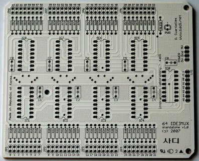
This board is exactly what I want to achieve, only mine has some more muxes.
One can see that there are not only capacitors between Vin and GND on the ICs, but also every IN of each IC has a Resistor connected between the IC-pin and the input-hole.
Now I have a couple of questions:

1) for what reason are there those resistors?

2) what values should those debouncing capacitors and the resistors have?

3) does it make a difference if some muxes poll analog and other digital signals?

4) in the middle between the two IC-rows, there is this horizontal lane with these holes ... is this A,B,C, INH ? .. if so, why are there so mane holes? and what could be the reason for placing them in the middle instead of outside like the other pin-holes?

5) on the power-pins on the right, it seems like there are two holes for GND.. as the whole GND-lane is thicker, can it be, that there are two cables with GND to connect here?

6) this pcb is for 8x 74HC4051, but there is a additional 4051 on the right, where the OUTs from the 8x 4051 are connected to.. is this a kind of "best practice"? .. my original plan was to connect all the OUTs directly to Teensy.
 
Hi

I try to make my multi-mux-board to work reliable. First I wanted to ask what capacitors I would need to debounde the IC itself and then I found this here:

View attachment 13829

This board is exactly what I want to achieve, only mine has some more muxes.
One can see that there are not only capacitors between Vin and GND on the ICs, but also every IN of each IC has a Resistor connected between the IC-pin and the input-hole.
Now I have a couple of questions:

1) for what reason are there those resistors?

2) what values should those debouncing capacitors and the resistors have?

3) does it make a difference if some muxes poll analog and other digital signals?

4) in the middle between the two IC-rows, there is this horizontal lane with these holes ... is this A,B,C, INH ? .. if so, why are there so mane holes? and what could be the reason for placing them in the middle instead of outside like the other pin-holes?

5) on the power-pins on the right, it seems like there are two holes for GND.. as the whole GND-lane is thicker, can it be, that there are two cables with GND to connect here?

6) this pcb is for 8x 74HC4051, but there is a additional 4051 on the right, where the OUTs from the 8x 4051 are connected to.. is this a kind of "best practice"? .. my original plan was to connect all the OUTs directly to Teensy.

1) From The looks of it those are either pull-up or pull-down resistors for buttons

2) The resistor can vary, it seems 10k is a fairly standard value that is used for buttons. Here’s a link to a page about the decoupling capacitors: http://www.thebox.myzen.co.uk/Tutorial/De-coupling.html

3) It does not matter from my experience:
09CBBDB4-3985-48BF-88EA-4418D48E84AE.jpg 3618AEF2-102C-40E6-9309-F143AAEA65DB.jpg
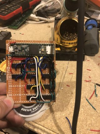
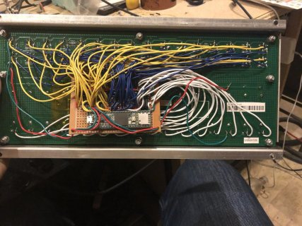
The first photo is a similar board used in the next photo where I have 32 buttons with leds and 16 slide potentiometers running side by side.

4) As far as I can tell this board is meant to be a standalone pcb so it didn’t need the A, B, C, and inhibit lines broken out to the outside. The holes are vias so that the address and inhibit lines can be ran to the multiplexers on the opposite side of the pcb.

5) It looks like there is two ground holes just so that he didn’t have to splice the grounds from the 5v and 9v power supplies somewhere else.

6) It doesn’t seem as if this is meant for another multiplexer, but rather for another micro controller that is only 16 pins (I can think of an ATTiny84, however it’s only 14 pins). You can tell because on the right side where it says I/O that’s the extra pins left over from the micro controller after all the multiplexers are connected to it.
 
1) From The looks of it those are either pull-up or pull-down resistors for buttons

2) The resistor can vary, it seems 10k is a fairly standard value that is used for buttons. Here’s a link to a page about the decoupling capacitors: http://www.thebox.myzen.co.uk/Tutorial/De-coupling.html

3) It does not matter from my experience:
View attachment 13835 View attachment 13836
The first photo is a similar board used in the next photo where I have 32 buttons with leds and 16 slide potentiometers running side by side.

4) As far as I can tell this board is meant to be a standalone pcb so it didn’t need the A, B, C, and inhibit lines broken out to the outside. The holes are vias so that the address and inhibit lines can be ran to the multiplexers on the opposite side of the pcb.

5) It looks like there is two ground holes just so that he didn’t have to splice the grounds from the 5v and 9v power supplies somewhere else.

6) It doesn’t seem as if this is meant for another multiplexer, but rather for another micro controller that is only 16 pins (I can think of an ATTiny84, however it’s only 14 pins). You can tell because on the right side where it says I/O that’s the extra pins left over from the micro controller after all the multiplexers are connected to it.

Hi , thank you for the answers :)

1) but don't those pull-resistors disturb analog redings?

3) very nice :) .. but I can't see that you have decoupled the ICs itself (?)

4) this makes sense with point 6)

5) do I understand it correctly that GND is GND no matter what current Vin has?
 
Hi , thank you for the answers :)

1) but don't those pull-resistors disturb analog redings?

3) very nice :) .. but I can't see that you have decoupled the ICs itself (?)

4) this makes sense with point 6)

5) do I understand it correctly that GND is GND no matter what current Vin has?

1) The resistors are there on the pcb if you want to add them for buttons, but you don’t need them there for the analog signal to go through.

3) When I made this I didn’t have any capacitors so I didn’t decouple any of them but I took it in to consideration as I made it.

5) In a sense yes, if you have to connect two power supplies into a circuit the grounds need to be connected together at some point.

great.. thank you very much :)
 
Status
Not open for further replies.
Back
Top