
You are using an out of date browser. It may not display this or other websites correctly.
You should upgrade or use an alternative browser.
You should upgrade or use an alternative browser.
Teensy 4.0 Schematics/eagle files?
- Thread starter capt.asic
- Start date
defragster
Senior Member+
Paul posted recently to a similar post - they are on his list of things to be done ASAP. It has been noted that his Schematic creation is manually created for usable detail - not just spit out from other software.
https://forum.pjrc.com/threads/57112-Teensy-4-0-Release?p=211727&viewfull=1#post211727
https://forum.pjrc.com/threads/57112-Teensy-4-0-Release?p=211727&viewfull=1#post211727
PaulStoffregen
Well-known member
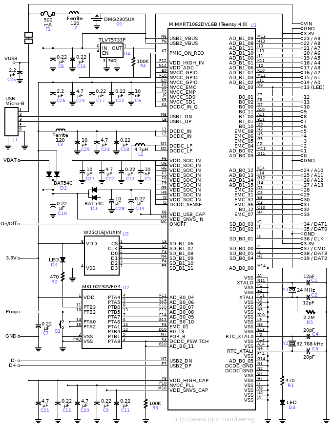
I'm drawing the schematic now. It's going to take a while...
But here's the GPIO part. Hopefully no big surprises?

But here's the GPIO part. Hopefully no big surprises?
dukeblue219
Active member
I'm drawing the schematic now. It's going to take a while...
But here's the GPIO part. Hopefully no big surprises?
View attachment 17242
Paul, it looks like you've got a typo there. B1_00 is tied to 7 and 8 on your diagram.
PaulStoffregen
Well-known member
Opps, a typo indeed.
Here's the completed schematic.
Also on the schematics page:
https://www.pjrc.com/teensy/schematic.html
Here's the completed schematic.
Also on the schematics page:
https://www.pjrc.com/teensy/schematic.html
defragster
Senior Member+
Is that lowly switch on the mkl02 the famous Teensy *TM* Brickproofing Button?
Valid assumption that those many extra mkl02 pins {versus T_3.x's} are somehow related to what might be a debug avenue once noted?
Valid assumption that those many extra mkl02 pins {versus T_3.x's} are somehow related to what might be a debug avenue once noted?
PaulStoffregen
Well-known member
What’s the DMG2305UX’s function?
Reverse polarity protection
PaulStoffregen
Well-known member
Added minor fixes to the schematic, for the Program pin and 3.3V & GND (right side of the board between On/Off & VTAB). Also added 10 of the 11 test points which were overlooked earlier.
PaulStoffregen
Well-known member
Indeed, N12 (USB_OTG1_CHD_B) is floating. That open drain output pin would normally be used to integrate the USB charger detection to an external power management chip, presumably so it could know when to draw much more current. Sorry, Teensy 4.0 doesn't support that sort of external power management integration. The wakeup pin (L6) and standby request (L7) are also unconnected.
PMIC_ON_REQ is connected to the 3.3V regulator enable, but that's the extent of Teensy 4.0's support for hardware power management. Trade offs had to be made to fit everything into the small size. Many other features (like native ethernet) that people wanted didn't make the cut either.
PMIC_ON_REQ is connected to the 3.3V regulator enable, but that's the extent of Teensy 4.0's support for hardware power management. Trade offs had to be made to fit everything into the small size. Many other features (like native ethernet) that people wanted didn't make the cut either.
PaulStoffregen
Well-known member
Valid assumption that those many extra mkl02 pins {versus T_3.x's} are somehow related to what might be a debug avenue once noted?
Nope, not really. This new chip has several complex features which required extra pins. That's all.
Why didnt you just upload the schematic from your CAD software?
Maybe because he is not using a CAD SW?
I'm curious how you would build a custom board without using some form of software to design it")
Have a look at https://forum.pjrc.com/threads/3525...d-board-layout?p=108451&viewfull=1#post108451
Conclusion, if you know your business post-it is all you need!
PaulStoffregen
Well-known member
In this case, I upgraded from the usual post-it notes to a full letter-size sheet of paper with notes about each BGA pin. Even used Robin's collection of many different colored highlighter pens. She's a huge fan of color coding stuff. I usually don't bother, but this was a bigger project.
Still, no CAD software for the schematic. Sure, a schematic is useful for communicating with others. But for just me, as 1 guy without anyone else on the engineering "team", CAD schematics just slow me down.
Still, no CAD software for the schematic. Sure, a schematic is useful for communicating with others. But for just me, as 1 guy without anyone else on the engineering "team", CAD schematics just slow me down.
MichaelMeissner
Senior Member+
Have a look at https://forum.pjrc.com/threads/3525...d-board-layout?p=108451&viewfull=1#post108451
Conclusion, if you know your business post-it is all you need!
There is an urban legend that states Apple bought a Cray whatever to help design their next computers doing layout, etc. while Seymour Cray is said to have replied that he used his Apple Mac (or whatever was the current machine) to draw the diagrams, etc. to design the next Cray.
PaulStoffregen
Well-known member
you have N11 twice, I think you meant N14 on the VDD_ADC_3v3.
Yes, you're right. Thanks for noticing! I've updated the schematic.
Also fixed the pins for the USB1 signals, which were off by 1 row.
semielectron
Member
Hello Paul,
I have a few questions related to the schematic and how open source teensy would be in general.
1- Is the schematic of teensy 4 or 4.1 available in any of the layout software such as eagle or Altium?
2- If I want to make the custom Teensy, is the bootloader code will be available?
Thank you
I have a few questions related to the schematic and how open source teensy would be in general.
1- Is the schematic of teensy 4 or 4.1 available in any of the layout software such as eagle or Altium?
2- If I want to make the custom Teensy, is the bootloader code will be available?
Thank you
semielectron
Member
Thanks for the quick response.
Do you know how much does it cost for the bootloader?
Thank you
Do you know how much does it cost for the bootloader?
Thank you