I2C Communication

Status
Not open for further replies.
Hi,
I wanting to begin using the i2c protocol and have a few basic questions. Does anyone know if i2c offers the same (10 Bit) resolution that normal analog pins do?
 
The I2C bus is used to transfer data in the form of bytes. What data these bytes represent is up to you to define.
The term resolution thus is irrelevant.
If you are connecting a sensor that has say a 16 bit resolution, then you'll have to transfer 2 bytes. For a bus system the term data rate, or how much data per time unit can be transferred is more of a measure.
 
Thank you for the answer. I do see some conflicting information about data rates for i2c, is it defined by the microcontroller (teensy in this case) or the i2c protocol or the i2c device itself? It looks like 100kHz is the standard data rate which corresponds to about 15 kBytes/second, do you concur?
 
It depends on your device as well as on the microcontroller.

Most halfway recent I2C bus capable devices can run up to 400KHz. Newer devices often follow the FM+ spec that allows up to 1MHz of I2C bus frequency. The Teensy3 can run FM+ frequency well in excess of 1MHz. There is an alternative I2C library here on the forum that will allow to to run the Teensy3 up to 1.8MHz.

The IO of the Teensy3 incl the I2C bus runs at 3.3V. Be mindful of that when designing your project.

Perhaps you state what you want to build and we go from there as there can be a few more caveats depending on your project requirements ;-)
 
In I2C, the master device (the one which initiates the communication) controls the clock speed. The slave device can hold the line low to lengthen (slow) the clock pulses, so the speed is not always as fast as you might expect purely from the clock rate.

The Wire library defaults to using 100 kHz when you use it as a master.
 
Thank you both for the information. Basically I have sensors that I am trying to read now that Firmata has support for i2c, and it looks like Maxuino has added some i2c functionality that I am looking to explore.

One sensor I am trying to read is the ADXL-345 accelerometer. From Sparkfun "digital output data is formatted as 16-bit twos complement and is accessible through a I2C digital interface"

This is confusing as I have only used the ADXL accelerometers with analog pins (analog data).

Do you have any suggestions on how to read i2c data with firmata? ( http://firmata.org/wiki/V2.2ProtocolDetails#I2C )
 
Seems to me that this ADXL should be pretty simple to interface with, the issue rather is the sheer number of registers you will have to familiarize yourself with (see page 23). The manual over at Analog devices has a section dedicated to I2C as well as SPI communications. Keep in mind that the CS pin on the chip has to be tied high for I2C communications to work. Additionally, the pullup resistors on SCL/SDA are also important. Other than that, interfacing this thing with a Teensy 3 should be trivial since both are running at 3.3V.

Get a hold of a I2C sketch for a similar, but simpler, ADC like the MCP3221 series so you can familiarize yourself with how I2C works on the Arduino/Teensy. Then I recommend you sit down and learn the basics of two's-complement math, bit-shifting operations, etc. if you don't know them already in order to make it easier to set and manipulate all the values that can be set in those registers. Finally, write a init routine to set up the chip to your liking, and a read routine to monitor the chip routinely. You could use the PIT timer library to periodically sample the chip or use the interrupt pin to alert the Teensy that another conversion has completed.

FWIW, I would use the interrupt to drive your read cycles and any pin on the Teensy 3 can be set to be an interrupt. Unless the math is very simple, I only set a flag inside the interrupt routine (i.e. "conversion complete") and the next time the CPU passes by the "something to read?" fork, it reads the ADC value(s).)
 
Last edited:
I take opportunity to continue on this post for a short question realted to IMU and I2C bus.
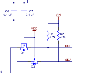
In the datasheet of an IMU board, I cannot understand this connections:
Bildschirmfoto2.png.
The board should work with 5V (Vin) and 3.3V (Vdd) systems, but it seems that using the Vdd (3.3 V) both resistances of 4,7 kOhm are bypassed (see Q1, Q2).
To me, if I use Vdd both resistances are disconnected from both lines.
It should not be a resistance on SCL and SCA even if the board or a sensor is powered by 3.3 V??


Here a short connections explanation:
Using the AltIMU-10
Connections

A minimum of four connections are necessary to use the AltIMU-10: VIN, GND, SCL, and SDA. VIN should be connected to a 2.5 V to 5.5 V source, GND to 0 volts, and SCL and SDA should be connected to an I²C bus operating at the same logic level as VIN. (Alternatively, if you are using the board with a 3.3 V system, you can leave VIN disconnected and bypass the built-in regulator by connecting 3.3 V directly to VDD.)
Pinout
PIN Description
SCL Level-shifted I²C clock line: HIGH is VIN, LOW is 0 V
SDA Level-shifted I²C data line: HIGH is VIN, LOW is 0 V
GND The ground (0 V) connection for your power supply. Your I²C control source must also share a common ground with this board.
VIN This is the main 2.5 V to 5.5 V power supply connection. The SCL and SDA level shifters pull the I²C bus high bits up to this level.
VDD 3.3 V regulator output or low-voltage logic power supply, depending on VIN. When VIN is supplied and greater than 3.3 V, VDD is a regulated 3.3 V output that can supply up to approximately 150 mA to external components. Alternatively, when interfacing with a 2.5 V to 3.3 V system, VIN can be left disconnected and power can be supplied directly to VDD. Never supply voltage to VDD when VIN is connected, and never supply more than 3.6 V to VDD.

The data ready and interrupt pins of the LPS331AP, L3GD20, and LSM303DLHC are not accessible on the AltIMU-10; if you need these outputs, consider using our LPS331AP carrier, L3GD20 carrier, and LSM303DLHC carrier boards.

The above schematic shows the additional components the carrier board incorporates to make the LPS331AP, L3GD20, and LSM303DLHC easier to use, including the voltage regulator that allows the board to be powered from a single 2.5 V to 5.5 V supply and the level-shifter circuit that allows for I²C communication at the same logic voltage level as VIN. This schematic is also available as a downloadable pdf: AltIMU-10 schematic (193k pdf).
I²C Communication

The LPS331AP’s barometer, the L3GD20’s gyro, and the LSM303DLHC’s accelerometer and magnetometer can be queried and configured through the I²C bus. Each of the four sensors acts as a slave device on the same I²C bus (i.e. their clock and data lines are tied together to ease communication). Additionally, level shifters on the I²C clock (SCL) and data lines (SDA) enable I²C communication with microcontrollers operating at the same voltage as VIN (2.5 V to 5.5 V). A detailed explanation of the protocols used by each device can be found in the LPS331AP datasheet (453k pdf), the L3GD20 datasheet (2MB pdf), and the LSM303DLHC datasheet (629k pdf). More detailed information about I²C in general can be found in NXP’s I²C-bus specification (371k pdf).
The barometer, gyro, accelerometer, and magnetometer each have separate slave addresses on the I²C bus. The board pulls the SA0 pins on the gyro and barometer high.

In our tests of the AltIMU-10, we were able to communicate with all three chips at clock frequencies up to 400 kHz; higher frequencies might work but were not tested. The chips themselves and carrier board do not meet some of the requirements to make the devices compliant with I²C fast mode. They are missing 50 ns spike suppression on the clock and data lines, and additional pull-ups on the clock and data lines might also be necessary to achieve compliant signal timing characteristics.
 
Last edited:
Status
Not open for further replies.
Back
Top