
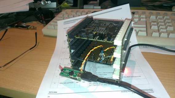
The Teensy++ 2.0 I am using is still running at 5V, the SGTL5000 has max voltage (including/espeically IO) of 3V6 and I have taken some care to make successful connections between GND, SDA & SCL on the devices without being too naughty, I'll happily detail how I think I've done that more than the code or picture I (intend to) attach to this post does if asked.
I appear to have basic control over the SGTL5000, config changes I make to VAG and VDDD measure appropriately - I drive VDDD to 0.8V and read pin 30 on SGTL5000 as very close to that value, change VDDD to 1.6V and sure enough the voltage on pin 30 is very close to the new value again, same with other offset voltages for various pins on the device.
I can route LINE IN to HEADPHONE directly by outputting 0x40 to CHIP_ANA_CTRL which appears to concur with the datasheet but nothing I have tried so far has made the source traverse the DAC, ie., pathway LINE IN->DAP->DAC->LINE OUT hasn't seen the source fed to LINE IN appear at LINE OUT in any way shape or form for me in quite a few hours of playing with this.
After much experimentation and wonderment I found that bits 12 & 13 (VOL_BUSY_DAC_LEFT & VOL_BUSY_DAC_RIGHT) are always set in CHIP_ADCDAC_CTRL no matter what I do, from the first moment I can query the register thru every attempted config change right to the final moment of letting my shoulders fall and shaking my head again.
The datasheet (http://cache.freescale.com/files/analog/doc/data_sheet/SGTL5000.pdf?pspll=1) says that those two bits have reset condition of 0x0 (termed that way in datasheet on page 34) but every time I power cycle (minimum 5 seconds off) the 'project' and make my first read of that register I get 0x323C which also indicates RSVD bits 7:4 are not in their stated reset condition of 0x0 either
The attached code is perhaps ugly/rudimentary/already-spaghettifying but it appears to function well enough, it makes input like ">0xe,0x200 <0xe" do the writing and reading of registers in the SGTL5000 and output like "Write 0xE=0x200 (newline) Read 0xE=0x3200". It also accepts "I" as the command to do my current idea/version of the initialisation sequence for SGTL5000 with values applying as follows;
CHIP_LINREG_CTRL,0x8
CHIP_ANA_POWER,0x7260
CHIP_LINREG_CTRL,0x60
CHIP_REF_CTRL,0x1F1
CHIP_LINE_OUT_CTRL,0x322
CHIP_PLL_CTRL,0x8000 (Edited in: I know I am not actually employing the PLL, this is a harmless (imho) leftover from an experiment I tried)
CHIP_CLK_TOP_CTRL,0x8
CHIP_ANA_POWER,0x57FF
CHIP_DIG_POWER,0x70
CHIP_CLK_CTRL,0xA
CHIP_ANA_CTRL,0x4
CHIP_SSS_CTRL,0x30
CHIP_ADCDAC_CTRL,0x200
DAP_CONTROL,0x1
I don't think it is really Teensy++ 2.0 support question but Paul has played with SGTL5000 before and I wrote to Freescale support 2 days ago, no reply yet; I posted to tower geeks forum yesterday and nobody read my post last I checked a few mins ago - I think they might be being snobs over the fact that I am not using any of their processor boards for tower thing; I was handed the bits I have (aside from my Teensy++ 2.0) as 'free bits', just in case you are wondering
I already feel pretty embarrassed over this so don't spare my feelings, please just tell me where I've gone wrong if you can
Attachments
Last edited: