After *much* thought & consideration, I'm 90% confident we're going to use the Freescale MK66FX1M0 chip for a Teensy++ 3.x product.
Freescale's website has complete specs and documentation for their MK66FX1M0 chip. Some highlights: 180 MHz Cortex-M4F (single precision FPU), 1M Flash (with 8K cache), 256K RAM, 4K EEPROM, 2 USB ports, ethernet, SDHC, 2 ADCs (many pins muxed), 2 DACs, 3 SPI, 4 I2C, 2 CAN, 6 serial, 20 PWM, touch sensing.
We'll almost certainly skip the first generation of Cortex-M7 chips and then consider making a Cortex-M7 board when the next generation arrives. As much as I've wanted to go with Cortex-M7, every indication is the first generation will offer only modest performance improvement that will likely come as a high cost increase. I believe the "sweet spot" for Cortex-M7 will arrive farther in the future, as the semiconductor vendors move to under-90nm silicon processes for microcontrollers. In the meantime, this new MK66FX1M0 chip will let us get a high-end Teensy done relatively quickly. My goal is to get this done by Christmas. Of course, everything always takes longer than expected, so please don't consider this as hard deadline. It's more of an optimistic goal.
")
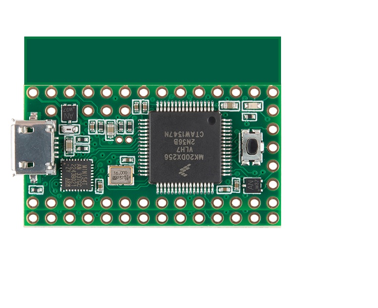
My plan is a 48 pin form factor board, where the left-side 28 pins exactly replicate the existing Teensy 3.1 & LC form-factor. The extra space on the right hand side will be mostly used for a SD card and some sort of connector for a 2nd USB port.
These chips have about 90 available I/O pins. Only about half will be able to come to the breadboard-friendly edges. I haven't decided what we'll do with the others. A high density connector is unlikely. I'll probably try to bring as many useful signals as I can to bottom side pads, similar to Teensy 3.1. Only one thing is absolutely certain: difficult compromises have to be made!
The K66 chip has an ethernet mac. I intend to bring all the RMII pins to the edges, so an ethernet shield can be made. Good software support for the on-chip ethernet port may take a very long time, but I do want that to be a long-term option, so we're almost certainly going to use the K66 chip instead of the K26.
One minor downside is that none of these newer chips offers 5 volt tolerance.
The other change is power consumption. For speeds above 120 MHz, the chip uses a special "high speed run" mode, which consumes quite a bit more power. It's looking like approx 90 to 100 mA. If the 2nd USB port is used, quite a bit of extra current is required for 480 Mbit/sec speed.