Question about vias

Status
Not open for further replies.

Constantin

Well-known member
For those of you that design PCBs, I have a silly question: why do some PCB manufacturers allow vias to touch / intersect with SMD component pads, while others do not?

I have been using iTead for a while, and I've been under the impression that the shorter the better re: any connection to a ground plane. Hence I have been using two 13 mil vias with every GND pad for a decoupling capacitor for example to connect it to the GND plane on the other side of the pcb.

However, the design rules for OSH PARK consider this a no no. Compliant designs require that GND pads are not intersected / touched by vias.

So why is it that iTead can make a PCB with a via that touches the solder pad while OSH Park objects to this approach? I am sure there is a reason... And should I change my boards to reflect the OSH PARK way?
 
There a distinction between what the PCB fab allows, and what your CAD software allows.

OSH Park does indeed allow drill holes anywhere within the outline of your board. When you submit files, you're just sending shapes and drill locations. They does some basic checking to figure out the outline of your design, but really, that's about it. You can submit pretty much anything.

But most CAD tools have design rule definitions that prevent you from drawing things that aren't expected to work. If you're not able to draw something, odds are good it's happening entire in the CAD software. Of course, most of those rules have rationale why drawing such a thing might be a bad idea. In the case of vias inside SMT pads, for reflow soldering, this usually results in unreliable connection because some or all of the solder flows down the hole, leaving little or no solder to join to the bottom side of the SMT part.

If you _really_ want to do that anyway (perhaps for a part you know will be hand soldered), it is possible. You just need to figure out how to make your CAD software actually do it.
 
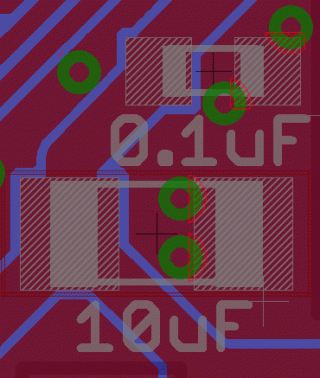
Interesting and thank you! FWIW, the drawing is in Eagle, checked once with a Design Rule (DRU) file from iTEad, the other time with a DRU file from Osh Park. The only difference is the DRU file being applied to check the boards... and the Osh Park DRU check results in hundreds of violations... I've never had a visible amount of solder squeeze through a 13mil via but I understand why it could be a problem at larger diameters.

GND Via.gif

FWIW, the centers of the GND vias in question are not inside the pad area, just their associated rings. Via rings intersecting with the pad show up as a clearance issue in Eagle when using a Osh Park DRU file (see bright red hatched areas). The clearances required by OSH Park around vias / pads also appear to be somewhat larger.

It's papers like this one and this one and finally this one, that suggested the Via / pad overlap to me in the first place as a means of minimizing inductance. I'm also looking into X2Y caps for signal conditioning and perhaps even decoupling.

Thank you again, Paul.
 
Last edited:
Having the via's too close to the pads can lead to reflow issues. The capillary effect of the vias can suck away the solder and when the vias are not small enough, gravity can pull the solder through and and out of the via.
Referring to this slide "Via Configuration Can Change Inductance" i'd use the "Best" approach with the vias located toward the inside still connected via little leads. If it does not lead to reflow problems ther should be no reason you could not have these rings overlapping. I don't think it will prevent you from generating the Gerber's for production.
 
Thanks Headroom, I appreciate your help!

I'm likely just lucky. Presumably, as I use boards with a HASL surface finish, I've gotten away with it since the holes will get stuffed by the Sn/Pb dip. But if I ever switch to ENIG (like Laen uses at Osh Park), then perhaps a 13 mil hole is big enough to allow some solder to creep/slip/slide from the pad. Thanks for the heads up!

Time to revise those pads... and make sure they only touch the via rings at most! Thanks again.
 
Last edited:
I think the issue is the layers you have selected, turn some layers and I'd guess most of those errors will go away. The likely problems are 29-30 and 39-43. Those are not Osh Park errors. I put holes in the pads under QFNs and Osh builds them with no problems.

Ira
 
Hi Ira and thanks for the suggestions!

I turned off every layer above 29 and still got the errors. Then I turned off more layers and discovered they're all layer 1 errors, i.e. Top.
 
You're right, the difference is on clearance tab of the DRC dialog. Osh has same signal spacing set to 6 and Itead has it set to 0. It's more a setting for you, as that will not effect Osh's ability to make a PCB for you. That check is is more about design standards and either he neglected to change it from the defaults or left it to help his customers make fewer mistakes. I just mark those as accepted and let them stay. But the earlier comments were correct, if you're going to go to production, you should talk to your vendor about choices like that. If the hole is small often the solder mask on teh other side will fill it and prevent problems. Also putting the hole in the middle of the pad might allow the paste to fill the hole before soldering and solve the wicking problem. But, I've not done this yet in production so it's possible I've made some serious error in judgement.

Ira
 
Status
Not open for further replies.
Back
Top