
I'm a little new to Teensy-ville, but not hardly a noobee. I decided to lay out my own custom pcb for the 3.1 module. I've seen some of the available BOBs, but want something more "permanent" and hard-wired. I do Arduinos a lot, and for some time have been wanting an Arduino UNO sized board with the power of the Teensy, and that could mount regular shields.
Basically the pcb layout is about 98% complete already, but I'm not sure about several pins. I did look all over the PJRC website, and did google searches,
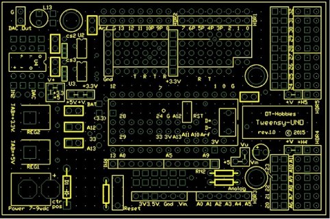
1. the pcb Reset switch is tied to Program pin, with no external pullup.
2. D33 is not to be used for input [per a forum thread].
3. so far, A12 and A13 are not tied to anything - TBD.
4. every other I/O pin is tied to a header, and with series-protection Rs on
all the digital pins, and voltage-dividers on the ADC channels.
5. the power to Vin [module 28] can come from either the Vusb pin or the
5V, 1A regulator on the pcb, via a jumper.
6. I also have a 3.3V, 1A regulator on the pcb, which is NOT tied to the
module 3.3V; the module 3.3V is not used to power any pcb peripherals,
except the pullup-Rs on ADC 4,5, when used for I2C.
7. There are also 2/ea SOIC8 SPI chips for RAM or EEPROM, and an opAmp
for the DAC, plus a small proto area.
The question is, is there anything special about A12, A13, or any of the other pins besides D33 that needs some sort of special attention? Is there anything special I should know about mounting shields, other than the usual 5V to 3.3V issues.
Overall, there is too much going on with the processor for me to figure it all out myself. Thanks.
Basically the pcb layout is about 98% complete already, but I'm not sure about several pins. I did look all over the PJRC website, and did google searches,
1. the pcb Reset switch is tied to Program pin, with no external pullup.
2. D33 is not to be used for input [per a forum thread].
3. so far, A12 and A13 are not tied to anything - TBD.
4. every other I/O pin is tied to a header, and with series-protection Rs on
all the digital pins, and voltage-dividers on the ADC channels.
5. the power to Vin [module 28] can come from either the Vusb pin or the
5V, 1A regulator on the pcb, via a jumper.
6. I also have a 3.3V, 1A regulator on the pcb, which is NOT tied to the
module 3.3V; the module 3.3V is not used to power any pcb peripherals,
except the pullup-Rs on ADC 4,5, when used for I2C.
7. There are also 2/ea SOIC8 SPI chips for RAM or EEPROM, and an opAmp
for the DAC, plus a small proto area.
The question is, is there anything special about A12, A13, or any of the other pins besides D33 that needs some sort of special attention? Is there anything special I should know about mounting shields, other than the usual 5V to 3.3V issues.
Overall, there is too much going on with the processor for me to figure it all out myself. Thanks.
Attachments
Last edited:
") .
.