Custom build Teensy 3.1 PCB not responding

Status
Not open for further replies.
Hi Constantin,

thanks a lot :). Do you know why Paul did connect I2C between both ICs? In the "official" schematics both are connected together. Thanks for the info with the 5x5 QFN. Sounds great. When I started the project I have been a poor hand soldering type guy, but I recently bought a toaster oven with controller that is just awesome. My next project will use the 5x5 QFN.

Best,
Phillip
 
Due to popular demand I have created a simple "reference board" for a custom Teensy 3.1 in EAGLE CAD format.

I've added a link on the Mini54 page.

Would you allow me to put the image of your board on the Mini54 page too? Showing the image could really help attract attention to your link, since that page is filled with lots of other text and links.
 
Do you know why Paul did connect I2C between both ICs?

LOL, I know why.... it was an early idea for someday supporting USB host mode. You can safely omit those 2 connections. At this point, I'm 100% certain that feature I will never use those 2 wires.
 
I have removed the I2C connection from my "reference" board. Thanks for clearing things up. Perhaps you want to use the updated image (board is online now without the I2C connection)

Phillip
 
Hey that's awesome!

My work still hasn't let me do this (waiting for approval to publish....) and my only comment is that the two lines going from the bootloader to the I2C headers on the MK20 are not needed. Simplifies things somewhat and takes 3 seconds to do. The 5x5mm QFN bootloader chip also needs fewer capacitors, is smaller, and requires no via transitions to be implemented. Helps on a more common 2-layer board!

Hope you are well and thank you for contributing this and your other musings on app fruit. I hope you participate in the wiki when the time comes because you have made some really good observations on your blog. Cheers, Constantin

What do you mean with "The 5x5mm QFN bootloader chip also needs fewer capacitors, is smaller, and requires no via transitions to be implemented"?

Do you mean that the trace has to be on the same layer using direct conneciton? If i understood this ok, what is the matter for such a guideline?

Thanks!
 
Hi Phillip,

I used your schematic as a starting point and have just assembled my first pcbs and of course they don't work. One thing I noticed after the fact that on Paul's schematic the Mini54TAN has pins 17 and 32 connected to GND but not on your schematic. Do you know why the discrepancy and could this be the reason I don't seem to get the K20 programmed by the Mini54TAN?
 
Hi,

my schematic and design uses the TQFP version of the Mini54TAN and not the QFN variant. Both have different pin setup. Have a look at this page:
https://www.pjrc.com/store/ic_mini54_tqfp.html

Required Connections:
--------------------

Code:
TQFP    QFN    Signal     MK20XXX Pin
----    ---    ------     -----------
 38      26     P0.0      MK20 Pin 23 (PTA1)
 33      22     P0.6      MK20 Pin 25 (PTA3)
 34      23     P0.5      MK20 Pin 25 (PTA3)
 32      21     P0.7      MK20 Pin 22 (PTA0)
 37      25     P0.1      MK20 Pin 24 (PTA2)
  9       7     P3.4      MK20 Pin 38 (PTB3)
 10       8     P3.5      MK20 Pin 37 (PTB2)
  8       6     P3.2      MK20 Pin 34 (Reset)
 20      13     P5.2      Program Pushbutton
 42      28     VDD       +3.3V
 43             AVDD      +3.3V (TQFP only)
 25      17     P2.5      Ground
 47      32     P1.4      Ground
 17      12     VSS       Ground
  5             AVSS      Ground (TQFP only)
 18             LDOCAP    0.1uF Capacitor to Ground (TQFP only)
         33     VSS       Ground (QFN only, connect center pad to ground)

All other MINI54 pins should be left unconnected

I really hope that is not the reason as this would probably render your PCBs completely useless (two much wires to reroute).
 
Last edited:
Thanks for the reply.

It looks like I got confused when I mated my 4x4 MINI54TAN package to an existing symbol and inadvertently left the GNDs at P2.5 and P1.4 off the schematic. This can't be good so I will have another revision made. I am also going to add test points as you suggested since using my oscilloscope probe proved unwieldy without them and I even damaged some of the flimsy K20 pins (poor soldering!).

At least my boost converter is producing 3.25 V. I got something right!

I might try to connect these pins to GND and see if I can make this board work but it is just a matter of time to get new boards made.

And thanks for the very useful how-to page and diagnostic info, without it I would not be as far ahead as I am!
 
Onehorse, did you use my eagle libraries for the bootloader and the MK20 chips in question? Just want to make sure I didn't overlook something. the GND pins on the DFN should have been defined as such...
 
Yes, I (mis) used your library. I made my own MINI54TAN package for the 4 mm x 4 mm QFN since I didn't find one there then lazily adapted on of the existing symbols. I forgot to check with Paul's schematic and just assumed it was about right. But the one I chose was missing the P2.5 and P1.4 GND connections. I noticed other symbols had the four GND connections combined. In any case, I redid the schematic and have submitted a new board to OSH Park.

What I still don't know, is this omission enough to cause the bootloader to fail to upload to the K20 or is there still some design error lurking for me to find?
 
IIRC, I never published a QFN 4x4mm version of the miniTan, just the 5x5mm one, hence confused I am. I never did find a proper 4x4mm DFN package with the right number of pins, so I stopped with just the TQFP and the 5x5mm version.

I highly recommend switching to the MKL02 bootloader for the simple reason that you get a small package with a low pin count (i.e. greater pin-pin pitch). Makes soldering all the more reliable and the extra pins on the MiniTan weren't used anyway.
 
I bought ten of each thinking I would start with the Teensy 3.1 and then transition to the Teensy 3.2.

I don't have a problem soldering the 4mm x 4 mm QFN, the Invensense MPU9250 is worse and I've successfully soldered hundreds of these (unsuccessfully a couple!).

I am happy to share my MINI54TAN 4mm x 4 mm package/symbol/component but I would recommend anyone interested in using this part to just make their own, it is not too hard.

I wish I had followed my own advice!

Anyone know whether leaving P2.5 and P1.4 floating could be the cause of my misdaventure to date?
 
What do you mean with "The 5x5mm QFN bootloader chip also needs fewer capacitors, is smaller, and requires no via transitions to be implemented"?

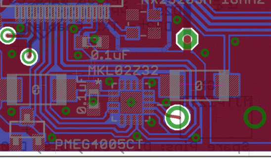
It means that I was able to implement the smaller bootloader chip without the need for vias when connecting to the MK20 on a 2-layer board. I happen to suffer from a bit of OCD when it comes to maintaining a unbroken GND plane on one side of my 2-layer designs. The smaller QFN chip is hence easier to implement for me. I didn't get so lucky with the MKL02 bootloader version. Note how it features two 0-Ohm jumper resistors.
 

Attachments

  • Bottom.gif
    Bottom.gif
    87.3 KB · Views: 170
Just thought would show a little as well as tell.

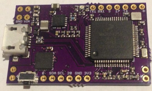
This is the board I put together that doesn't work:

Teensy.jpg

you can recognize this as a modified version of Phillip Schuster's reference design.

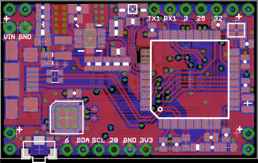
and this is what the revision will look like:

Teensy2.brd.png

You can see I've added test points to better diagnose what else goes wrong...

My ocd manifests as a desire to wring every last square mm of space out to make the smallest board possible. Haven't really got started here yet since I need to just make it work, but i am aiming for another 10% reduction with more components to add...
 
Last edited:
That's very cool. Is this a 4 layer board or 2? If 2, I wonder to what extent you may also be having issues with the crystal not being happy on account of the GND plane around it. In the image above, you can see how I have moated the crystal, the two crystal lines are the same length (measured in eagle) and a crystal GND plane surrounds the crystal, joins the two GND pads of the crystal, then goes under the MCU and joins the crystal GND to the GND pin there. The GND return path from the 0.1uF decoupling capacitor to MCU GND is separate (i.e. the GND from the crystal joins underneath the MCU, the crystal GND joins from the outside). That way, the GND path to the crystal will never feature junk from the decoupling cap and vice versa.

I can see why you chose to put the bootloader where you did but I prefer mine as close to the pins in question as possible. Hence what you see above.
 
It's great to see my work used :). And as it's so great to see I have more:

Just if you are interested: Today I made my project that I have been building with the custom Teensy open source! I also did write an extensive blog post describing various design decisions, full schematics and layouts, BOM, 3D model for the enclosing and the whole source code. Take it as a reference or inspiration or just build a Little Helper yourself. It's a very useful small device and is a lot of fun to use.

Take a look: http://www.appfruits.com/littlehelper
 
Is this a 4 layer board or 2?

It is four, with a GND and 3V3 plane beneath the xtal then some components below. I'm not too happy about the latter but it is a compromise for small size. But the inner layers should shield well enough. I don't think this is the problem but maybe a problem later on. But this xtal and this kind of layout work well on the nRF51822.

I am hoping it is the missing GND pins on the MINI54TAN that is my problem. I will know in a couple of weeks.

Thanks again Phil, your blog was/is enormously useful. If there is to be a Teensy wiki I hope you have a prominent how-to section there. If I ever get my board to work I will consider similarly posting a how-to/lessons learned write up. I think we ought to make it as easy as possible to customize Teensy applications.

In fact, we ought to be able to define guaranteed-to-work reference designs as you have done for both 2- and 4-layer boards with a list of known-to-work components, etc. Maybe a bit ambitous...
 
When I built my custom Teensy the main issue I had was selecting parts? Which part to choose for the ferrite beads, etc. I tried to choose parts that are widely available and added MPNs to the Eagle board so everyone has a jump start and must not do the same things I did.

My new custom Teensy design "Little Helper" linked above is one step ahead by providing schematics, layout and describes various parts of the design and why I chose to do it that way. I hope that really helps everyone to get started with a custom Teensy project as this project is not only a reference board for getting Teensy up and running but also shows more complex power supply support for battery powered devices and how powerful this can be.

I am interested to hear what you think about it.
 
I think the more detailed information about the choices you made and why the better for those who might follow; only most custom builds will have different constraints. Mine does.

BTW, I noticed that most custom Teensy builds do not use load caps on the 16 MHz xtal. On the nRF51, the pin capacitance is ~1 pF so to match the 8 pF Xtal capacitance I use 12 pF load capacitors. I also used these on my custom Teensy board. But if the K20 pin capacitance is 4 or 5 pF, load caps greater than 6 or 8 pF might cause the Xtal to misbehave. I wonder if this is what could be preventing the K20 from running on my board?
 
There must be a reason that Paul does not use load caps - and there is allways the chance to adjust the K20 internal caps via register write.
 
Yes, I was just looking at the rather longish K20 manual; it appears external load caps are not required. I will try to replace them with 1 pF caps or zero Ohm resistors and see if my Teensy comes to life!
 
Yes, I was just looking at the rather longish K20 manual; it appears external load caps are not required. I will try to replace them with 1 pF caps or zero Ohm resistors and see if my Teensy comes to life!

I didn't follow the whole thread, but are you suggesting replacing load caps on a crystal oscillator with shorts (0 ohm)? You'd short out everything to ground...:confused:
 
Status
Not open for further replies.
Back
Top