Constantin
Well-known member
Hi Paul,
I did something sacrilegious the other day, I 'extracted' a MKL02Z bootloader chip from a existing LC board to find a new home on a MKL26Z-based power measuring device I am trying to develop. I'm so excited re: trying out the LC chip in this capacity that I couldn't wait, sorry!
However, try as I may, the thing isn't responding when plugged into the USB port (i.e. it doesn't enumerate). I found no shorts with my multimeter, and then I went over my schematics twice and found no error there either (vs. the posted schematic).
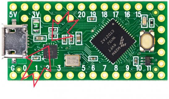
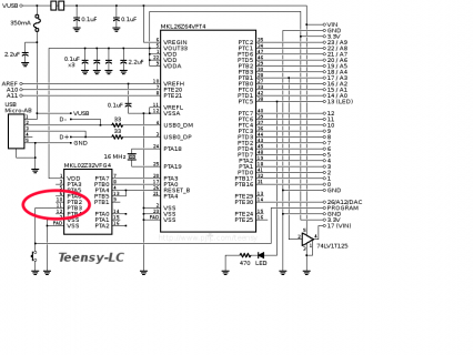
Today, I thought I'd compare the posted pic of the Teensy LC vs. the schematic (thank you for posting that!) and I wonder if I may have found an error in the posted schematic vs. the actual board shown here.
Note how on the bootloader chip there is a connection at pin 10 (the top red arrow) but no apparent connection on pin 11 (the bottom arrow)

I suspect that the PGM button is attached to pin 10 in real life and not pin 11 per the schematic (see below). On the off chance that I'm right, would you recommend simply jumpering the two pins with a blob of solder, or does the MKL02Z dislike that? (i.e. in case pin 11 is not high-Z by default like most of the pins on the MK20)

I'm not home now to test the connections with a multi-meter and I am more than happy to be wrong... so please accept my apologies in advance if I am! But sight unseen, I'm willing to bet an ice cream sandwich that pin 10 is attached to PGM. Anyone want to take me up on that wager?
Or can someone use a multimeter to see if pin 10 of the bootloader is electrically attached to one side or the other of the PGM button? Or that pressing PGM causes pin 10 to go to GND?
Note: This potential error, if it is one, will not affect anyone except those who want to roll their own Teensy LC. Currently, you'd have to scavenge a LC boot loader off an existing board or wait until PJRC starts shipping them individually. Thus, even if this turns out to be an errata, it does not affect pre-assembled boards from PJRC.com. Buy a few and enjoy them - I know I do!
I did something sacrilegious the other day, I 'extracted' a MKL02Z bootloader chip from a existing LC board to find a new home on a MKL26Z-based power measuring device I am trying to develop. I'm so excited re: trying out the LC chip in this capacity that I couldn't wait, sorry!
However, try as I may, the thing isn't responding when plugged into the USB port (i.e. it doesn't enumerate). I found no shorts with my multimeter, and then I went over my schematics twice and found no error there either (vs. the posted schematic).
Today, I thought I'd compare the posted pic of the Teensy LC vs. the schematic (thank you for posting that!) and I wonder if I may have found an error in the posted schematic vs. the actual board shown here.
Note how on the bootloader chip there is a connection at pin 10 (the top red arrow) but no apparent connection on pin 11 (the bottom arrow)

I suspect that the PGM button is attached to pin 10 in real life and not pin 11 per the schematic (see below). On the off chance that I'm right, would you recommend simply jumpering the two pins with a blob of solder, or does the MKL02Z dislike that? (i.e. in case pin 11 is not high-Z by default like most of the pins on the MK20)

I'm not home now to test the connections with a multi-meter and I am more than happy to be wrong... so please accept my apologies in advance if I am! But sight unseen, I'm willing to bet an ice cream sandwich that pin 10 is attached to PGM. Anyone want to take me up on that wager?
Or can someone use a multimeter to see if pin 10 of the bootloader is electrically attached to one side or the other of the PGM button? Or that pressing PGM causes pin 10 to go to GND?
Note: This potential error, if it is one, will not affect anyone except those who want to roll their own Teensy LC. Currently, you'd have to scavenge a LC boot loader off an existing board or wait until PJRC starts shipping them individually. Thus, even if this turns out to be an errata, it does not affect pre-assembled boards from PJRC.com. Buy a few and enjoy them - I know I do!
Last edited:

