Request: Castellated Edges on Teensy 3.1 PCB

Status
Not open for further replies.
I can't see why you can't make a surface footprint for Teensy 3.1 PCB on your PCB, paste your PCB (including apertures in the stencil for Teensy 3.1 pads), run it through the auto-loaders in your line (if any) and then hand place the Teensy 3.1 PCB - pop it in the reflow oven (probably best if you use low-melt solder paste and take care to set the oven as low as possible to flow it) and inspect.

If connecting to the pads on the underside of Teensy which do not have holes I would be inclined to place plated-thru holes on my 'mother' PCB to mate with them, I would make the hole size (after plating) be the small dimension of the rectangular pads - expecting this would make it a bit easier to determine if it connected well or not without xrays. I expect I might have a bit of a fight on my hands, getting the stencil made right, because nobody in their right mind has apertures over holes :D
 
I do think that Paul should (and he probably does) took a good look at Particle/Spark. They are just a little easier to embed into other projects I think.
 
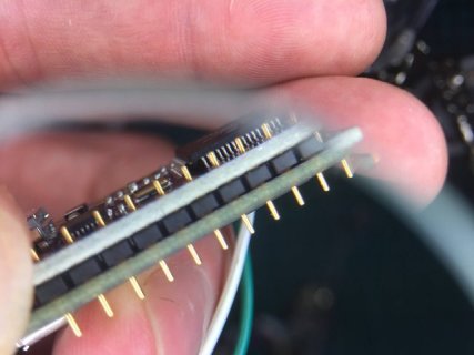
types of edge castellation

I found that photo interesting. I have seen the board edge cut through the center of a through-hole, making it SMT mountable but preventing through-hole pin use. Slicing along a smaller chord of the through-hole allows use of the PCB either with TH or SMT mounting, which I have not seen before. I guess that places some more stringent accuracy requirements on the edge routing.

castellated-edges.png

If you do mount it SMT style, the unfilled holes make nice test points for probe tips as well.
 
Can't this be done DIY with a good router, a bandsaw, or one of those guillotine-Style paper cutters at the office?
 
Last edited:
Someone actually cut down and posted success here. They were trying to fit a Teensy in tube. I don't know/recall if all the pins were still usable after cutting.
 
Maybe with a guillotine-style metal shear at the fab shop. I'm doubtful of a good outcome with the other suggestions. With care and patience, also a hand file.
 
A razor saw like this would probably work, but it would be rough on the blade. You can also get mitre boxes for this kind of saw.
 
...I'd confirm first though if there are any important traces running on the outside of the pin holes. :)
 
Paul posted on the thread with the guy fitting a Teensy into a tube that no traces go outside the holes, but there are traces running parallel to the hole centerlines, so going to the hole edges works, going more than half way through the holes risks pulling traces. Do like the partly cut holes for SMT soldering, though the mechanical strength as a through hole device would be lower.

Of course if you are hand modding Teensy's for multi unit project the hours involved start pushing more to a 'teensy on a PCB' integrated solution. Unless OneHorse makes a Teensy Teensy with a BGA.
 
I recall that post, he used a file it seems with teensy in a padded vice
I was wondering if the little thin steel blade <3" chop saw would cut clean, works well on brass tube.
 
If the teensy is flat enough (i.e. no RTC on the underside), I wonder if some round pads with solder paste would not be enough. A hot air rework station would provide the localized heating...
 
I'm not sure if this is possible with V-score PCB edges.

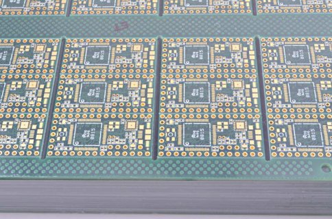
Here's a photo of some Teensy 3.1 circuit boards, before assembly:

panels.jpg

As you can see, we use tab routed slots to create the left and right edges. The top and bottom are V-score. Our contract manufacturer uses a machine with a big cutting wheel to separate the boards. It looks like a big pizza cutter. It follows the score line and separate the boards.

I'm not sure if this castellated edge feature is even possible with boards separated this way. The photos I've seen look like the PCBs were fully tab routed.
 
@PaulStoffregen I'm pretty sure you'd have to switch to fully routing the boards with "mouse bites" probably to hold them together as a panel. That would probably add more cost. Maybe consider it for your next design?

In my case, that would let me make a SmartMatrix Shield that could be assembled using a hot plate, for customers that don't want to spend the 15-30 minutes to solder it themselves, or don't have the soldering skills/tools. It would be a good option between a bag of parts kit and a custom board using the MINI54.
 
With a proper jig would this 2" saw I referred to do the job clean enough to open the pin holes?
http://www.harborfreight.com/2-in-mini-bench-top-cut-off-saw-61900.html

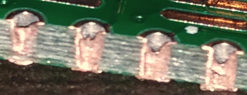
I spent more time on photo than cutting - held this to a wood scrap with a screwdriver - the copper wiped over:
choppcbs.jpg
BTW: My saw doesn't even come up to speed right after many hours of use and that same blade may have cut through 4,000 plus pieces of brass.

I got a castellated onehorse 9DOF board I put under the T_3.1 using solder paste with a hand iron. I wonder the success rate of soldering a through pin or two then pasting the other holes and putting in the oven?
 
Last edited:
I'd wager an ice cream sandwich that if you come up with a pad representation of the Teensy underside (i.e. a round pad for every hole, a rectangular pad for every underside pad, etc.) that you could reflow the teensy right onto a new board, no cutting required. In fact, you may even get good connections to the Pogo-pin receptacles like D+, D-, reset, etc.

I'd wager a further ice cream sandwich that a hot plate approach with a good stainless stencil for the paste is more than good enough to get the job done, as long as you align the teensy well each time (maybe use header pins in opposite corners to fix the thing in place, then snip off the excess when done).

The reason I'd look into the hot plate vs. using an oven is to lessen the stress of the components on top. I.e. cook the PCB below vs. cooking the Teensy components up top. Or in a reflow oven, you could simply disconnect the top emitters and only heat from below. At some point in the future, I'll do just that, i.e. use that dual SCR I have in mine to selectively turn on and turn off heaters above and below. The idea being that the quartz lamps below are great for initial baseline and soak while the top quartz come on for the quick rise to reflow temperatures.
 
I recently designed a small breakout board, using through hole vias, with which you solder directly through the vias on the breakout board to the teensy. Just apply a little solder on one side, flip over and do the same on the other side. It seems to make solid connections (although granted, I've only soldered two of them up so far). I used this methodology in order to break out the pads on the bottom too, then the whole lot connects to a pair of parallel 2mm headers, which allows me to breakout all of the T3.1 pins, without increasing the footprint dramatically.

Unfortunately, the design was done at work and so I can't share it, however. "/ When I next solder one up, I'll grab a couple of pictures though to demonstrate it properly.
 
Last edited:
As I recall, the Schmartboard folk do something similar to allow you to solder the big GND pad on the underside of a QFN chip.

Another approach could be to use through-holes throughout on the breakout, hand apply solder paste to every pad/pin of interest on the teensy (i.e. bottom facing up) then place the breakout above and use a hot air gun to melt the paste. The capillary action would have the paste come up into the via, showing when it's done. The downside to this approach though (vs. the hotplate) is likely much longer time needed to get the job done (with all the temperature-related issues like stress on the components). That's why I'd go for the one and done approach with a hot plate.
 
Is thete a castellated version of teensy 3.1? This is my thought of a castellated teensy 3.1:
1. The pcb thickness should be 0.1mm
2. Square shape at least 25mmx25mm
3. Pitch at least 1mm
4. All pins must be exposed

I hope we can vave a teensy like this, can it handle androud wear? No pins pn the underside, mich better to have the rtc parts soldered already.
 
Last edited:
Looking at the V-score picture, I can't help wondering if rotating the T3.1s by 90 degrees would enable castellation on the two long edges of the board.
 
Is thete a castellated version of teensy 3.1? This is my thought of a castellated teensy 3.1:
1. The pcb thickness should be 0.1mm
2. Square shape at least 25mmx25mm
3. Pitch at least 1mm
4. All pins must be exposed

A 0.1mm PCB thickness does not seem attainable unless you want something that breaks at a moments notice.
 
Maybe he meant 1.0 mm? 0.1 mm is thinner than many flex cables. I measure a Raspberry Pi camera flex cable (which has only a single trace layer) around 0.12 mm in the middle and 0.33 mm at the ends where the stiffener is.
 
Last edited:
Smart watch,
iTead charges extra for anything below 1.0mm in two layers and the lowest they go is 0.8mm for 4 layers. Granted, PJRC use a higher-quality supplier than the iTead fab, but I can't imagine that 4 layers can be done in anything approaching 0.1mm barring NSA-like budgets. At 1oz of outer and ½ oz inner copper trace layer thicknesses, that comes out to 0.09mm just for the copper, leaving you a scan 0.002mm for each layer of insulation. Good luck with that! ;)

Especially if the idea is to reflow a Teensy on top of a new board, I'm unconvinced that going thinner is better. I'd wager that a thicker (i.e. 1mm and up) board would do better at resisting warping at reflow temperatures than a skinnier one. But I don't have scientific evidence to back it up... I just know that I much prefer a 1.6mm thick board to a 1.0mm board on account of how much more reliable / solid / etc. pin holes are in the thicker stock.

As for the square form factor, I wonder how that's supposed to breadboard compatible. Paul has been shaping his Teensys this way for a long time and I doubt he's going to deviate. My suggestion would be to go roll your own if you have very specific requirements. For example, few users need access to ALL pins... I'm perfectly happy not leading the pins from the boot loader to the MCU rather than attempt to have access to the EZPort or SWD bus.

But that's the beauty of having access to all the required hardware. Build your own clone and resell it on tindie, etc. If the design is compelling you may even recoup your development costs. But don't forget that users also expect technical support, etc.
 
Last edited:
Status
Not open for further replies.
Back
Top