SEGA Megadrive/Genesis YM2612 + SN76489 synth

Status
Not open for further replies.
Howdy! That's my code, lol. I saw a YouTube comment about this thread and popped on over.

In order to use a Teensy 3.1 you'll need to level shift (3.3v -> 5v, single direction (write only) ) the 8 bit data bus and pins A0, A1, /RD, /WR, and /CS

It might be easiest to replicate a single YM2612 connected to a Teensy 2.0 or Teensy++ first, and then get the Teensy 3.1 working. I have not yet upgraded my device to a Teensy 3.1 because I haven't had the time. The 2.0 is fine for most things a synth would do but has trouble keeping up with playing back VGM files - reading and writing the embedded PCM data from a VGM file over USB or Serial is more than it can handle in real-time.

My code is heavily dependent on the ability of the Atmel chip to change the state of an entire bus (8 pins per bus on the Teensy 2) by using the PORTA, PORTB, etc. registers (or whatever those are). Basically you can do something like PORTD = 0x5 to set pins 1 and 3 high and all other pins low on bus D. This reduces the number of instructions you need to provide to manipulate the data bus dramatically and simplifies your code.

I believe the Teensy 3.1 also has busses that can be manipulated the same way, but I recall them having strange widths (one of them was like 4 bits wide, another was like 16 I think?) and may require some experimentation or advice from an ARM guru to get right.

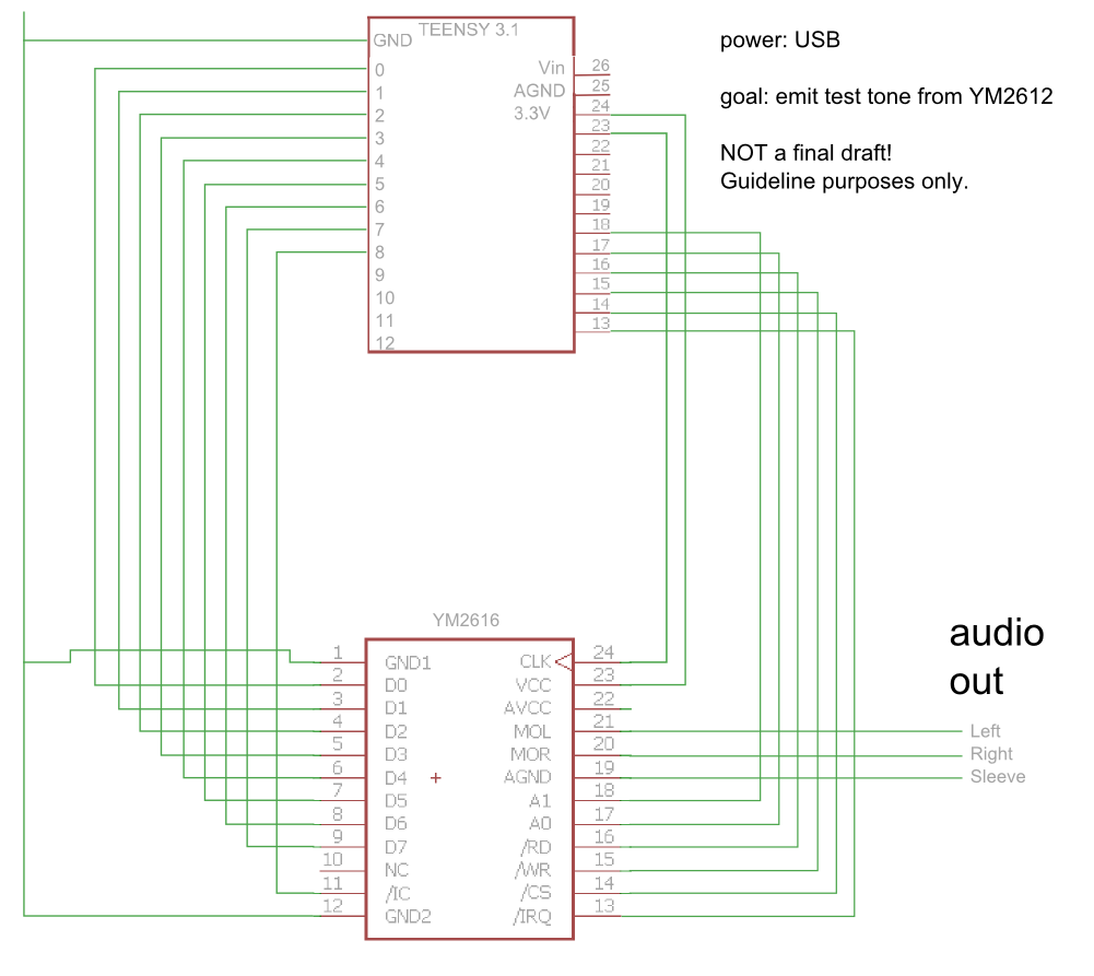
Here's the schematic of the hardware that works with that code:
WodUFd8.jpg

edit: forum mangulated the image, here's an imgur http://imgur.com/WodUFd8.png
 
Last edited:
Also sorry about not splitting out the different functions of the code into separate C files and stuff, I realize it's very hard to read. I didn't really know what I was doing when I wrote it.

Oh, by the way, you do NOT plug the YM2612 directly into speakers. You can do this for testing, but eventually this will damage the chip. It does NOT like impedance on the output stage and will heat up significantly. The original MegaDrive had a little headphone amp on the output, and the newer models (without the volume slider) had an op amp buffer if I remember correctly.

Again, this is OK to use for testing if you do not want to be troubleshooting your output stage hardware at the same time as you are troubleshooting the rest of your hardware / software, but replace the test YM2612 with a fresh one or re-test the output with a scope to make sure it's not damaged before assembling it into a final product, because it's likely to become damaged from that.
 
Last edited:
Thanks!! That was your code then? I notice it's for a finished synth. I'm still struggling with the very basics. of everything.

is the YM2612 basically full of flipflop switches that hold their state until the program addresses and writes to a register? I am unsure one would change a single parameter on the synth such as Algorithm number for example.
would it go like this:

WR, $some.8.bit.hex.value, and then ??

I know 'registers' stand for a location of something, but i am drawing a blank as to if the register = address, and if an address or register equals a parameter or a parameter value.
in short, i don't know much. I have read things, but documentation is either too general (making references to stuff i already know that seem irrelevant when i am hoping to read something i dont know that will fill in the blank)

in other words, once i have my hands on a real live register, what do i do with it? let's say i want to set the feedback level on an operator or change an algorithm type. what sort of electrical events does my test program need to perform?

Yeah, it looks like i'm going to need to buy a ++ to get these 5v signals.

Does your code handle the 'register' stuff? i'm trying to write an 8 bit data bus code from scratch.

this is what i have so far:

Code:
#define YM_IC (13) // PC5 (= pin 13 for Teensy 3.1)
#define YM_CS (14) // PC4 (= pin 14 for Teensy 3.1)
#define YM_WR (15) // PC3 (= pin 15 for Teensy 3.1)
#define YM_RD (16) // PC2 (= pin 16 for Teensy 3.1)
#define YM_A0 (17) // PC1 (= pin 17 for Teensy 3.1)
#define YM_A1 (18) // PC0 (= pin 18 for Teensy 3.1)
#define YM_D0 (0)  // D0  (= pin 0 for Teensy 3.1)
#define YM_D1 (1)  // D1  (= pin 1 for Teensy 3.1)
#define YM_D2 (2)  // D2  (= pin 2 for Teensy 3.1)
#define YM_D3 (3)  // D3  (= pin 3 for Teensy 3.1)
#define YM_D4 (4)  // D4  (= pin 4 for Teensy 3.1)
#define YM_D5 (5)  // D5  (= pin 5 for Teensy 3.1)
#define YM_D6 (6)  // D6  (= pin 6 for Teensy 3.1)
#define YM_D7 (7)  // D7  (= pin 7 for Teensy 3.1)

I'm trying to "port" a simple test program from AVR to Teensy, here is the original with some stuff commented out:
of course it doesn't work at all because there are dependencies i don't have.
Code:
/**
 * YM2612 test code for AVR.
 * MODIFIED for TEENSYDUINO July.8.2015
 * This program is a simple test code for the YM2612 FM sound chip using an AVR ATmega328p mcu.
 * This program configure the YM2612 to sound like a "grand piano" and play note on / note off in loop.
 * For more informations about wiring please see: http://en.wikipedia.org/wiki/Yamaha_YM2612
 * For more informations about YM2612 registers please see: http://www.smspower.org/maxim/Documents/YM2612
 *
 * @remarks This test code is heavly based on Furrtek's YM2612 test code. Big thanks Furrtek for the help !
 * @warning This test code is made to run on an ATmega328/ATmega168 mcu with a 16MHz external crystal.
 * 
 * @author Fabien Batteix <skywodd@gmail.com>
 * @link http://skyduino.wordpress.com My Blog about electronics
 */

/* Dependencies */
#include <avr/io.h>     // For I/O and other AVR registers
#include <util/delay.h> // For timing

/* Pinmap (Arduino UNO compatible) */
#define YM_IC (13) // PC5 (= pin 13 for Teensy 3.1)
#define YM_CS (14) // PC4 (= pin 14 for Teensy 3.1)
#define YM_WR (15) // PC3 (= pin 15 for Teensy 3.1)
#define YM_RD (16) // PC2 (= pin 16 for Teensy 3.1)
#define YM_A0 (17) // PC1 (= pin 17 for Teensy 3.1)
#define YM_A1 (18) // PC0 (= pin 18 for Teensy 3.1)
#define YM_CTRL_DDR DDRC
#define YM_CTRL_PORT PORTC
#define YM_DATA_DDR DDRD
#define YM_DATA_PORT PORTD // Whole PORT D for data bus (= pins D0 to D7 for Arduino UNO)
//#define YM_MCLOCK (1) // PB1 = OC1A (= pin D9 for Arduino UNO)
//#define YM_MCLOCK_DDR DDRB

/* ----- BIG WARNING FOR ARDUINO USERS -----
 * Normally ICSP port is used to program the AVR chip (see the makefile for details). 
 * So, if you use an arduino UNO board to run this test code BE VERY CAREFULL.
 * If you don't known what you make you will be in trouble.
 *
 * To avoid problems you can compile and upload this code using the Arduino IDE BUT you will need to disconnect pins Rx/Tx before upload !
 */

/**
 * Send raw data to the YM2612
 * 
 * @author Furrtek
 * @param data Data to write
 */
static void write_ym(uint8_t data) {
  YM_CTRL_PORT &= ~_BV(YM_CS); // CS LOW
  YM_DATA_PORT = data;
  _delay_us(1);
  YM_CTRL_PORT &= ~_BV(YM_WR); // Write data
  _delay_us(5);
  YM_CTRL_PORT |= _BV(YM_WR);
  _delay_us(5);
  YM_CTRL_PORT |= _BV(YM_CS); // CS HIGH
}

/**
 * Write data into a specific register of the YM2612
 *
 * @author Furrtek
 * @param reg Destination register address
 * @param data Data to write
 */
static void setreg(uint8_t reg, uint8_t data) {
  YM_CTRL_PORT &= ~_BV(YM_A0); // A0 low (select register)
  write_ym(reg);
  YM_CTRL_PORT |= _BV(YM_A0);  // A0 high (write register)
  write_ym(data);
}

/** Program entry point */
int main(void) {

  /* Pins setup */
  YM_CTRL_DDR |= _BV(YM_IC) | _BV(YM_CS) | _BV(YM_WR) | _BV(YM_RD) | _BV(YM_A0) | _BV(YM_A1);
  YM_DATA_DDR = 0xFF;
  // YM_MCLOCK_DDR |= _BV(YM_MCLOCK);
  YM_CTRL_PORT |= _BV(YM_IC) | _BV(YM_CS) | _BV(YM_WR) | _BV(YM_RD); /* IC, CS, WR and RD HIGH by default */
  YM_CTRL_PORT &= ~(_BV(YM_A0) | _BV(YM_A1)); /* A0 and A1 LOW by default */
  
  /* F_CPU / 2 clock generation */
/* has dependencies that i apparently dont have */
TCCR1A = _BV(COM1A0);            /* Toggle OCA1 on compare match */
TCCR1B = _BV(WGM12) | _BV(CS10); /* CTC mode with prescaler /1 */
TCCR1C = 0;                      /* Flag reset */
TCNT1 = 0;                       /* Counter reset */
OCR1A = 0;                       /* Divide base clock by two */
  
  /* Reset YM2612 */
  YM_CTRL_PORT &= ~_BV(YM_IC);
  _delay_ms(10);
  YM_CTRL_PORT |= _BV(YM_IC);
  _delay_ms(10);

  /* YM2612 Test code */ 
  setreg(0x22, 0x00); // LFO off
  setreg(0x27, 0x00); // Note off (channel 0)
  setreg(0x28, 0x01); // Note off (channel 1)
  setreg(0x28, 0x02); // Note off (channel 2)
  setreg(0x28, 0x04); // Note off (channel 3)
  setreg(0x28, 0x05); // Note off (channel 4)
  setreg(0x28, 0x06); // Note off (channel 5)
  setreg(0x2B, 0x00); // DAC off
  setreg(0x30, 0x71); //
  setreg(0x34, 0x0D); //
  setreg(0x38, 0x33); //
  setreg(0x3C, 0x01); // DT1/MUL
  setreg(0x40, 0x23); //
  setreg(0x44, 0x2D); //
  setreg(0x48, 0x26); //
  setreg(0x4C, 0x00); // Total level
  setreg(0x50, 0x5F); //
  setreg(0x54, 0x99); //
  setreg(0x58, 0x5F); //
  setreg(0x5C, 0x94); // RS/AR 
  setreg(0x60, 0x05); //
  setreg(0x64, 0x05); //
  setreg(0x68, 0x05); //
  setreg(0x6C, 0x07); // AM/D1R
  setreg(0x70, 0x02); //
  setreg(0x74, 0x02); //
  setreg(0x78, 0x02); //
  setreg(0x7C, 0x02); // D2R
  setreg(0x80, 0x11); //
  setreg(0x84, 0x11); //
  setreg(0x88, 0x11); //
  setreg(0x8C, 0xA6); // D1L/RR
  setreg(0x90, 0x00); //
  setreg(0x94, 0x00); //
  setreg(0x98, 0x00); //
  setreg(0x9C, 0x00); // Proprietary
  setreg(0xB0, 0x32); // Feedback/algorithm
  setreg(0xB4, 0xC0); // Both speakers on
  setreg(0x28, 0x00); // Key off
  setreg(0xA4, 0x22); // 
  setreg(0xA0, 0x69); // Set frequency

  /* Program loop */
  for(;;) {
    _delay_ms(1000);
    setreg(0x28, 0xF0); // Key on
    _delay_ms(1000);
    setreg(0x28, 0x00); // Key off
  }
  
  /* Compiler fix */
  return 0;
}
 
Last edited:
Yes, my code does handle writing to the registers.

In the code you pasted in your last post, check out the selectreg3 function. It might be a little complicated, but it writes the data to the A0/A1/RD/WR/CS pins to select the appropriate register to alter.

The writereg3 function writes data to the currently selected register via the data bus.

The original selectreg and writereg functions are a little simpler, and they're still in the code. You can check those out too. Basically a YM2612 is split in half right down the middle - there are 6 channels, 2 of which (channel 3 and channel 6) are unique. Bank 1 controls channels 1-3, and Bank 2 controls channels 4-6. Channel 3 has a special mode it can (but not must) be put into in which it can generate multiple simple tones simultaneously. Channel 6 has a special mode it again can (but not must) be put into in which it no longer acts as an FM synth channel and instead is 8-bit PCM.

selectreg and writereg select and manipulate the registers for Bank 1, and selectreg2 and writereg2 select and manipulate the registers for Bank 2.

A register is a very small amount of storage space, kind of similar to RAM. When you select a register, you're essentially selecting the "parameter" to alter. When you alter the register, you're changing the parameter. So, when you select the register that controls "channel 1 operator 1 detune/MUL" and change the state of the detune, it's similar to physically turning a knob that controls that parameter.

Check out http://www.smspower.org/maxim/Documents/YM2612#partimemorymap and stare at it until you think it makes sense. Remember that the YM2612 is a 4-operator FM synth, and each operator of each channel can be controlled independently. Therefore, each operator for each channel has a uniquely-addressable register for each parameter, although most registers are actually overloaded and the bottom nibble or n bits controls one thing while the top nibble or n bits controls a different thing.

A0H+ and A4H+ are complex again because the LSB (least significant bits) and MSB (most significant bits) of the parameter that controls the note frequency are spread across two registers because the register size of the hardware is only 8 bits but Yamaha chose to use an 11-bit value for the frequency for some reason. To write this value, you need to jump through a couple hoops, but that's not so bad because you need to jump through some hoops to calculate the proper value in the first place, too.

To change the frequency, since it's more complex than any other register, I made the setpitch function (which is a pile of crap and really hard to read, as indicated by the 'wtf' comment, lol). Sorry about that, but again I didn't know WTF I was doing when I wrote this. Don't forget to actually play a note you have to twiddle the 'note on' register.

I recommend developing a strong working knowledge of how an ADSR envelope works and how basic FM synthesis and operator stacking functions in a Yamaha FM synthesizer before trying to parse this code in too much detail. There is a lot of info out there on how this works. If it seems overwhelming, don't forget that the primary criticism of the Yamaha DX synth line was that it was far too difficult for musicians to learn how to program.
 
(have you found a datasheet?)

Ha! And I say, 'Ha!' again!

The closest thing to a datasheet we have on this particular chip was obtained from a corrupt Word document salvaged from an email from a Japanese hardware engineer at Sega to an American hardware engineer named "sega2.doc". We've also found some datasheets (entirely in Japanese) from other OPL and OPN series chips that have similar implementations to the YM2612. All remaining information was obtained by trial-and-error and decapping the chip and taking microscope photographs of the physical transistors on the bare silicon!
 
If it seems overwhelming, don't forget that the primary criticism of the Yamaha DX synth line was that it was far too difficult for musicians to learn how to program.

here's some FM proof of concept by yours truly, a bit of software that does multichannel FM:

[soundcloud url="https://api.soundcloud.com/tracks/117788511" params="color=ff5500&auto_play=false&hide_related=false&show_comments=true&show_user=true&show_reposts=false" width="100%" height="166" iframe="true" /]


i bet the unknown stuff in the chip is a global phasemod coming from CV on pin10 (analog input as an FM modulator)
 
Last edited:
looks like the forum ate your soundcloud link :(

i bet the unknown stuff in the chip is a global phasemod coming from CV on pin10 (analog input as an FM modulator)

The register marked as "proprietary, do not use" in SEGA2.DOC is actually the SSG-EG register. See http://gendev.spritesmind.net/forum/viewtopic.php?p=5716#5716 for more info, scroll down to "YM2612: SSG-EG mode"

edit: And pin 10 is actually an output interrupt that asserts HIGH when the YM2612 is busy and LOW when it's ready to accept a write. You'll probably only need this if you attempt to overclock your YM2612 to write PCM at an unsupported sample rate, which has been done, with impressive results - here it is playing PCM at 44.1khz http://www.youtube.com/watch?v=fYWclV9H2eY. This is kind of silly though, I think the Teensy itself could have better PCM performance by itself than using the YM2612, lol. It kind of defeats the point of using a YM2612 in the first place, you lose the iconic pcm distortion.
 
Last edited:
looks like the forum ate your soundcloud link :(
soundcloud.com/amateurtoolsdsp/fm-life-js-mono-sound-example

The register marked as "proprietary, do not use" in SEGA2.DOC is actually the SSG-EG register. See http://gendev.spritesmind.net/forum/viewtopic.php?p=5716#5716 for more info, scroll down to "YM2612: SSG-EG mode"
ok...
edit: And pin 10 is actually an output interrupt that asserts HIGH when the YM2612 is busy and LOW when it's ready to accept a write. You'll probably only need this if you attempt to overclock your YM2612 to write PCM at an unsupported sample rate, which has been done, with impressive results - here it is playing PCM at 44.1khz http://www.youtube.com/watch?v=fYWclV9H2eY. This is kind of silly though, I think the Teensy itself could have better PCM performance by itself than using the YM2612, lol. It kind of defeats the point of using a YM2612 in the first place, you lose the iconic pcm distortion.

come to think of it, a teensy might just be made into a proper FM synth with the right software so its all redundant in a way eh? but nonetheless, i intend to figure this out :)
 
i've changed BUSPIN to 0 for the Teensy 3.1, (to use pins 0-7 for the 8bit bus) and I was looking for a way to change the pin numbers for the CS, WR, RD, A0, A1 things but couldn't discern them. I suppose that's PORTF on a Teensy ++.

i went ahead and tried to compile the code and I got the following errors, particularly interested in PORTF. What's that?

Code:
Arduino: 1.6.5 (Windows 7), TD: 1.24, Board: "Teensy 3.1, Serial, 96 MHz (overclock), US English"

ym2612_3.ino:69:68: warning: narrowing conversion of '-1' from 'int' to 'const unsigned char' inside { } [-Wnarrowing]
ym2612_3.ino: In function 'void input()':
ym2612_3.ino:147:8: warning: statement has no effect [-Wunused-value]
ym2612_3.ino: In function 'unsigned int readbus()':
ym2612_3.ino:170:8: warning: statement has no effect [-Wunused-value]
ym2612_3.ino:170:15: warning: assuming signed overflow does not occur when assuming that (X + c) >= X is always true [-Wstrict-overflow]
ym2612_3.ino: In function 'void selectreg(unsigned char)':
ym2612_3:189: error: 'PORTF' was not declared in this scope
ym2612_3.ino: In function 'void selectreg2(unsigned char)':
ym2612_3:208: error: 'PORTF' was not declared in this scope
ym2612_3.ino: In function 'void writereg(unsigned char)':
ym2612_3:263: error: 'PORTF' was not declared in this scope
ym2612_3.ino: In function 'void writereg2(unsigned char)':
ym2612_3:283: error: 'PORTF' was not declared in this scope
ym2612_3.ino: In function 'void keyUp(int, int)':
ym2612_3.ino:946:21: warning: comparison between signed and unsigned integer expressions [-Wsign-compare]
ym2612_3.ino: In function 'void writeram(short unsigned int, unsigned char*, unsigned int)':
ym2612_3.ino:1041:15: warning: comparison between signed and unsigned integer expressions [-Wsign-compare]
ym2612_3.ino: In function 'void readram(short unsigned int, byte*, unsigned int)':
ym2612_3.ino:1058:15: warning: comparison between signed and unsigned integer expressions [-Wsign-compare]
ym2612_3.ino:1051:8: warning: unused variable 'rec' [-Wunused-variable]
'PORTF' was not declared in this scope

  This report would have more information with
  "Show verbose output during compilation"
  enabled in File > Preferences.
 
Why do you think these pins are PORTF? CS, WR, RD, AO, and A1 aren't concepts that make sense from the point of view of the Teensy. Those are the physical pins on the YM2612.

PORTn registers are very much an AVR thing. Check out http://www.elecrom.com/2008/02/12/avr-tutorial-2-avr-input-output/ for a bit of an explanation.

The Teensy 3.1 is NOT an AVR chip and PORTn registers do not work the same way they do on a Teensy 2. PJRC has done some emulation of the PORTn registers of an AVR chip with the Teensy 3, though, and you can see it in avr_emulation.h in the core library. wibauxl on this forum made a good graphic that maps the ports to the pinout diagram here: https://forum.pjrc.com/threads/25643-Combined-Pin-Assignments-card

Altering this code to work with a 3.1 will be nontrivial and require knowledge of exactly what pins match to which ports and how to select the proper pins to use for your use-case.
 
Aah. My code's going to require significant effort to port to the 3.1 that I don't have time to focus on at the moment. Your schematic there can't physically work ever because you'll be driving the data bus at 3.3v

also you seem to be trying to supply VCC and A.VCC from data pins on the Teensy - this will kill your Teensy on the spot when you drive those 2 feet HIGH
 
Last edited:
Aah. My code's going to require significant effort to port to the 3.1 that I don't have time to focus on at the moment. Your schematic there can't physically work ever because you'll be driving the data bus at 3.3v

also you seem to be trying to supply VCC and A.VCC from data pins on the Teensy - this will kill your Teensy on the spot when you drive those 2 feet HIGH

nice catch, i threw that sketch together on inkscape because i dont know eagle yet.
i would definitely not connect it that way exactly. it would be wired differently! i need to erase that image!

you should probably have a read of this really useful port manipulation tutorial: https://forum.pjrc.com/archive/index.php/t-17532.html

thank you, will check it out.

im nowhere near getting this to go, i just want to get all the information out there so someone as dumb as me would understand ;)

EDIT, here's the updated probably wrong still schematic

jiBDHOd.png


I realize that T3.1 maybe underpowered for the job, i only want to get it most of the way there programwise. are all the pins going to be digital between the T3.1 and YM2612 aside from the power in and audio out and grounds?
 
Last edited:
EDIT, here's the updated probably wrong still schematic

...

I realize that T3.1 maybe underpowered for the job, i only want to get it most of the way there programwise. are all the pins going to be digital between the T3.1 and YM2612 aside from the power in and audio out and grounds?

yep, it's still wrong. here's just a few things:

1. voltage levels: ranix above has confirmed it won't work with 3v3 logic (unlike opl3), so assuming that's correct, you'll *need* level shifters of some sort or another. there's plenty of threads around here covering that and possible ICs, too; see here for the most recent one: https://forum.pjrc.com/threads/29135-Appropriate-Level-Shifting-IC-to-interface-Teensy-LC-to-5V-chip

2. power supply. you still power the yamaha chip via teensy, the 3v3 pin in this case -- which might even work if this was spec'd at 3v3. as per the unreadable ym2608 manuals, the ym2612 chip seems to want 4.75v (min), 5v (typical). so you'll need 5v from somewhere. Vusb might work for testing, which can be tapped from the Vin pin; in a proper application / synth you'd probably want a separate supply, proper decoupling (that's the caps you see on power lines), etc.

3. pins used. if you think you need the port thing, take a good look at the tutorial that i've linked, and that mortonkopf linked again. you'll note it goes on at length about "PORTD" in particular, saying that whereas PORTD (AVR) maps to "7,6,5,4,3,2,1,0 in that order, GPIOD maps to pins 5,21,20,6,8,7,14,2, in that order!"

so 5,21,20,6,8,7,14,2 are the pins you'd use with teensy 3 for the data bus. ie

T3.1 -> YM2612

pin 2 - > D0
pin 14 -> D1
pin 7 -> D2
etc

the same principle applies for the remaining pins (see the tutorial for a list). eg. GPIOC maps to pins 15 (C0), 22 (C1), 23 (C2), 9 (C3) ...
 
you really will need to get to grips with the port manipulation. Its not too difficult to understand once you leave behind the concept of adjacent physical pins being adjacent port pins. Ranix has said "My code is heavily dependent on the ability of the Atmel chip to change the state of an entire bus (8 pins per bus on the Teensy 2) by using the PORTA, PORTB, etc. registers ".
 
3. pins used. if you think you need the port thing, take a good look at the tutorial that i've linked, and that mortonkopf linked again. you'll note it goes on at length about "PORTD" in particular, saying that whereas PORTD (AVR) maps to "7,6,5,4,3,2,1,0 in that order, GPIOD maps to pins 5,21,20,6,8,7,14,2, in that order!"

if I get a Teensy++ then will the wires be in a linear order instead of being a big mess?

I've looked at the pinouts for it, and all the 'ports' are pinned out in a normal linear sequence.

This whole thing is giving me buyers remorse, of course I bought it with the idea that it was simply the most up to date one... I'm going to make this thing work even if I have to code it in wooden blocks and it takes 20 years.
 
The Teensy++ has several 8-bit wide ports and there's a lot of information on how to use them. You should be able to read up and eventually understand how to use them to communicate with a YM2612. The Teensy++ also operates with a native 5v supply and has 5v I/O. It will require no level conversion to communicate with a YM2612.

The Teensy 3.1 has several ports of varying widths and there are maybe 1 or 2 forum posts on how to manipulate them unless you can handle reading the 100+ page datasheet on the ARM processor itself. It may be over your head. I would personally take it seriously and dig in with a cup of coffee and a full day set aside to focus on porting my code to it. YMMV depending on skill level. The Teensy 3.1 has 3.3v I/O and will require unidirectional voltage conversion to communicate with a YM2612.

If I were in your shoes, it's somewhat unlikely that I would personally be able to port that code to the Teensy 3.1 without seeing it work on a Teensy++ first to simplify debugging. I wouldn't waste my time trying, it would probably take hours and a Teensy++ is a rather inexpensive part.
 
i'm having a hard time because i don't even know the first thing about teensy. i guess i need to know what ARM is, etc
 
Trying to hook up the yamaha chip is a very ambitious project, you dont have a full data sheeht for it, it is non trivial to communicate with it both physically due to voltage differences and protocol wise and you are using an unfamiliar micro controller to do it all.

An excellent first step would be to hook up a sn76489 to a teensy instead. It accepts 3.3v inputs (although it needs 5v on Vcc) and by default when you power it up it is generating a tone, so to get it to make a sound al you need to do is attach a 4mhz clock and power - job done no need for any microcontroller! Once you have it saying "booooooooooooooooooo" you ca attach the teensy and start playing with the very simple protocol to play different notes.

This way is a lot gentler than battling with the yamaha chip and you satisfying feed back early in the process.

but i have FIVE ym2612 chips... (good thing i also have five sn76489 chips too hehe)

thanks for the tip, will look into this now!
 
Status
Not open for further replies.
Back
Top