You are using an out of date browser. It may not display this or other websites correctly.
You should upgrade or use an alternative browser.
You should upgrade or use an alternative browser.
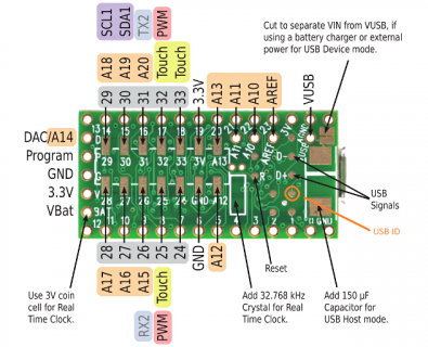
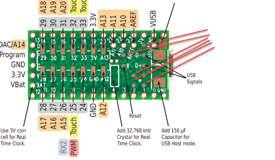
what are the pads under teensy 3.1 board?
- Thread starter doughboy
- Start date
- Status
- Not open for further replies.
Answering #2 first: Provided you connect correctly, yes, you can wire your own USB connection using those pads. Pretty sure 5th line is effectively for (at least simile of) chassis GND but I should probably review the schematic in question, maybe even consult my favourite EE, before saying that.
The unlabelled pads are used during programming and testing on Paul's bed of nails tester, pretty sure.
'Reset' does what it says, pulling it low will cause the MCU to restart.
The unlabelled pads are used during programming and testing on Paul's bed of nails tester, pretty sure.
'Reset' does what it says, pulling it low will cause the MCU to restart.
Pin 4 from the USB Micro is the ID signal. It is used for the USB Host mode/OTG, but currently not supported by the Teensy 3.1. Pin 4 can be left floating. The USB A Plug has only 4 Pins (VCC,DM,DP,GND) and no ID Pin.
How to repair a broken-off Teensy 3.0 USB connector
USB ID is one of the unlabeled pads:

The other unlabeled pads are for programming the MINI54 (ICE_CLK, ICE_DAT, /RESET) and from the K20: VDDA, VREGIN.
How to repair a broken-off Teensy 3.0 USB connector
USB ID is one of the unlabeled pads:

The other unlabeled pads are for programming the MINI54 (ICE_CLK, ICE_DAT, /RESET) and from the K20: VDDA, VREGIN.
Last edited:
PaulStoffregen
Well-known member
If you look at the schematic, you'll see those test pads are indicated as little dots on the ends of wires.
http://www.pjrc.com/teensy/schematic.html
The unlabeled ones are used during testing. We test every Teensy on a bed-of-nails test fixture. Spring loaded "pogo" pins touch each pad. The tester checks connectivity to all locations and lots of other stuff. Except for the USB connector, connectivity to every part of the board is tested.
Here's some info about the tester, from the Kickstarter when we launched Teensy 3.0 a few years ago.
https://www.kickstarter.com/project...rm-cortex-m4-usable-in-arduino-a/posts/305527
Teensy 3.1 has one more test pad, so a whole new bed of nail test fixture was made for 3.1. It looks pretty much identical to the older one in those photos.
Later in another test, we actually plug each Teensy in to USB cable and program the LED blink. That test verifies the USB connector, pushbutton and LED, which can't be tested by the bed of nail.
Thanks for the replies.
Any suggestions on how to cover up the unlabelled pads so there are no exposed contacts?
I don't really want to get solder mask paint unless that is the only option.
I'm thinking of using this technique
https://forum.pjrc.com/threads/2607...ns-with-a-socket?p=52894&viewfull=1#post52894
to connect the D+ and D- to a pin header without using specialized pogo pin, just like how it was done for the reset pad.
The D- will have one unlabelled pad in contact, and D+ has 2 pads that I need to cover/insulate from the pin header.
So the paint must be able to withstand 300C soldering iron heat.
Thanks!
pictographer
Well-known member
Cover the exposed contacts with Kapton tape?
Cover the exposed contacts with Kapton tape?
yeah, I found that on google search. I suppose I can either buy a roll of kapton tape or 5ml solder mask paint, they are both $0.99 each on ebay.
I'm just not sure if the added thickness of the tape will be a problem.
I can't see where this got corrected so I better correct myself this time: Pulling reset low halts the processor, releasing (or driving back high) the reset line will cause the processor to restart....
'Reset' does what it says, pulling it low will cause the MCU to restart.
- Status
- Not open for further replies.


