Teensy 3.2

Status
Not open for further replies.
I got mine from the last order from Oshpark and it's alredy on my Racecar tyre temperature sensor prototype !
I wonder Paul if after teensy LC you may consider doing an HC or pro version, i had a look on the K20 sub family and i've seen that a dual can channel version of K20 is avilable (MK20FX512VLQ12 price goes from 3$ to around 6$ in quantities according to Freescale) and for people like me using this hardware in the automotive market would be great to have a second can line.
Maybe a complete board is not even enecessay maybe just the support in the booloader and in teensyduino is enough then if you need the second can line you will just build your own board and buy the bootloader chip.
 
^ https://forum.pjrc.com/threads/24633-Any-Chance-of-a-Teensy-3-1

After *much* thought & consideration, I'm 90% confident we're going to use the Freescale MK66FX1M0 chip for a Teensy++ 3.x product.

Freescale's website has complete specs and documentation for their MK66FX1M0 chip. Some highlights: 180 MHz Cortex-M4F (single precision FPU), 1M Flash (with 8K cache), 256K RAM, 4K EEPROM, 2 USB ports, ethernet, SDHC, 2 ADCs (many pins muxed), 2 DACs, 3 SPI, 4 I2C, 2 CAN, 6 serial, 20 PWM, touch sensing.

Great times ahead for us CAN BUS geeks.
 
Last edited:
sounds pretty good, things i like about that chip mostly: MCU clock, FPU, SRAM amount and double the DAC, double the fun! :D
 
Homemade reflow oven + QFN?

The chip will be available in 2 sizes, the extremely small 3 mm QFN, and a large 7 mm TQFP with "easy" 0.8 mm pitch pins.

Hi

I know it's probably a bit OT to ask about this here but has anybody any experience with "homemade reflow oven" + QFN?

I've successfully made a custom build Teensy 3.1 with various chips down to 0.5mm pitch and 0603 parts. But all pins were visible/outside so far.

Also I had to remove quite a few bridges, so I'm a bit anxious about the hidden pins of QFN packages.

Hints about getting rid of bridges also welcome (it seems there is too much solder on the small pads, but barely enough on the big ones).

Thanks!

_Markk
 
All the time. Trick is not to put too much solder paste. But if you do then you can use a clean iron (absolutly no solder on the iron, so wipe it on a sponge again and again) and then just touch the bridge on the qfn. It should wick onto the iron.
If that doesnt work, try using a fine wire solder wick and gently and quickly tap the iron onto it. Becareful not to take to much solder away as you may disconnect the pin and then have to add solder again.
Finally if that doesn't work, you'll need some liquid flux usually in a dab pen form and dab the qfn, then get a hot air gun and yet the part till its lose and you should be able to gently move it in to position and hopefully de bridge.

Goodluck.
 
All the time. Trick is not to put too much solder paste. ... Goodluck.

Thanks for the answer but this is about using a DIY reflow oven with a solder paste stencil. I would never finish my design with hand soldering ;-)

CustomBuildTeensy.jpg

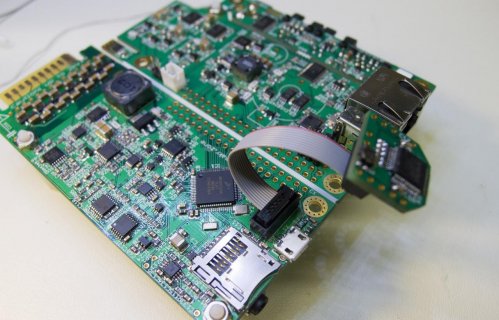
I hope I'll soon find time to start document the project. It's a Teensy 3.1 custom build + MCU controlled MPPT solar charger + weather station (wind speed, direction, rain, temp, humidity) + USB host with G3 modem stick and software PPP TCP/IP stack + simple audio amp/headphone + SD card + (the most important thing) gamma spectrometer with low power high voltage generator. It's my first design in electronics. Second PCB revision. And it's mostly working ;-) Third revision is in progress and I'd hate to introduce new problems...

-Markk
 
That was using a reflow oven. If you put to much pressure when squidging the solder paste through the stencil you'll get to much paste on the pads. Then when you reflow you may get bridges. What i described is how to fix after reflow.
Ive made a teensy+lipo charger+esp8266 micro board that uses these small qfn and sometimes when it comes out the oven it bridges because of inconsistent pressure when applying the paste through the stencil.
 
I find that most stencils (depends on the thickness) allow you to apply the correct amount of paste for qfn chips. It makes nice little balls when finished and I've never had too much solder.
Except I heat my boards with a hot air soldering gun.
 
That was using a reflow oven. If you put to much pressure when squidging the solder paste through the stencil you'll get to much paste on the pads. Then when you reflow you may get bridges. What i described is how to fix after reflow.

Ah, I completely misunderstood! Now that I reread after a good night of sleep it was obvious. Apologies.

Thanks for the tip about pressure because I obviously got it wrong, thinking I had not enough pressure for the stencil to really touch down on the BCP fully and therefore not scraping off enough. Will try lighter pressure next time.

About fixing after reflow thank you for the tips too. Judging from this, it seems QFN is no less likely to develop bridges than ordinary chips but also no more difficult to remedy...

BTW for others who may read this, in order not to repeat my mistake:

If you have solder bridges behind the legs of a chip (talking about outgoing pins, not QNF) you sometimes have to apply even more solder to really gobble it all up and only then wick it off. I destroyed a chip trying desperately to wick behind the legs, before I found this out >:-}

_Markk
 
Ah, I completely misunderstood! Now that I reread after a good night of sleep it was obvious. Apologies.

Thanks for the tip about pressure because I obviously got it wrong, thinking I had not enough pressure for the stencil to really touch down on the BCP fully and therefore not scraping off enough. Will try lighter pressure next time.

_Markk

Practically speaking, you can't apply too much pressure to the squeegee. Automated screen printers apply a substantial amount of pressure. What can happen is that the stencil bows up and allows too much past to flow sideways under the stencil leaving excess paste on the pads. It usually works well to tape tape the stencil to another piece of PCB material that is the same thickness as the target so it stays flat. Usually just under one side is enough but for the first few tries, it won't hurt to surround the target board with PCB material on all sides and tape the stencil to that. After you do it a few times, one side will probably be enough.

The thickness of the stencil also determines how much paste is left and 4-6 mils is fairly standard. Too much paste usually a bigger problem than too little.

It takes a little practice but you can always clean the board off and try it again.
 
Thanks veng1

What can happen is that the stencil bows up and allows too much past to flow sideways under the stencil leaving excess paste on the pads.

That's exactly what I thought. So on the second revision I pressed down quite hard. No change.

The thickness of the stencil also determines how much paste is left and 4-6 mils is fairly standard.

I ordered with Seeed and its a 0.12mm stencil, so ~4.7 mil.

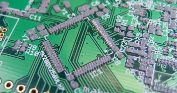
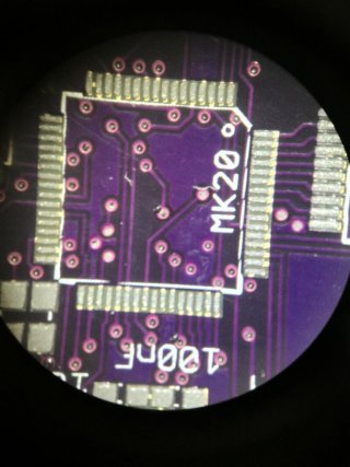
As I said I pressed down quite hard but it still looks way too thick:
Solder paste detail.jpg

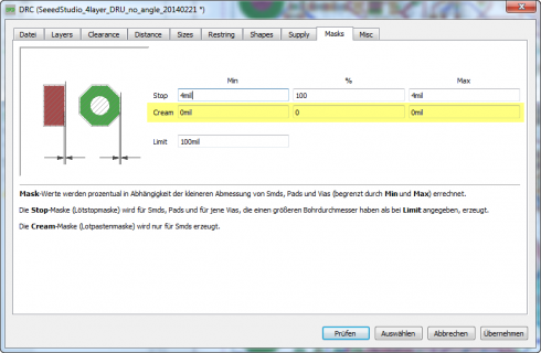
Perhaps it would help to reduce the cream layer outlines in relation to the smd copper in Eagle?
Eagle_DRC_Masks.png

Any suggestions welcome.

Thank you very much!

_Markk
 
Last edited:
I use the trick with old boards around the stencil too. Also makes it much easier to place the new board(s) correctly.

Markk: That thickness looks good to me.
If its only the processor that's bridging, I would look at the chip part library and make the creams smaller. Or reduce them globally as you're showing.
The problem with thinner stencils could be warping etc.
 
Normally the stencil house does a size reduction on the pads for small pads as the paste should be smaller than the pads, then a tombstone reduction where bigger SMT pads have a trapezoidal shape to pull the solder away from the center of the part to give good fillets and then on large pads like a voltage regulator or thermal pads a technique called a window pane is used to allow the flux gasses to escape.
 
There are two variables, the stencil thickness and the pad reduction.

I tend to use a thick stencil because I want the largest components I can get away with. I'll use a 0805 even if I could use an 0603 simply because it allows more process headroom independent of the fact that 0805 R's and C's cost more.

I then find a bigger stencil reduction allows the print to be offset more and still get a decent print but I'm coming from the direction where I want to max out a screen printer at 180 prints/hr, not by hand printing. It's not about how many prints you can get per hour, its about how many good prints you can get per hour. If 3 mils work you you, you should use it. If it ain't broke, don't fix it.
 
I tend to use a thick stencil because I want the largest components I can get away with. I'll use a 0805 even if I could use an 0603 simply because it allows more process headroom independent of the fact that 0805 R's and C's cost more.

Sorry for derailing this topic but how do thinner stencils require smaller parts? I haven't had any issues using e.g. 1206 LEDs or battery holders like this https://www.digikey.com/product-detail/en/BU2032SM-HD-G/BU2032SM-HD-GCT-ND/755451 with 3 mil stencils.
 
AFAIK, it's the other way around - parts with small pitches require thin stencils to prevent bridging. The downside is that thinner stencils (like the great mylar stuff that Osh stencils uses) will not last as long or be as durable. Also, I found that stainless stencils from the likes of itead tend to run on the thicker side. Great stencils but relatively thick, leading to somewhat common bridging for chips with high pitch densities such as the MK20.
 
Agreed. Thinner stencils give less paste thickness and will reduce bridging although somewhat of the same effect can be had be doing a stencil reduction where the stencil apertures are made smaller than the component pad thus also applying less paste.

Normally the thickness of a stainless steel stencil can be specified. I like to use SIPAD for prototypes as that includes the paste applied to the board, reflowed flat, tacky flux applied and then covered with a peel off film. Then the stencils they supply tend to work the same way in volume production. http://www.sipad.com/

With the SIPAD process, the film is pulled off and then the parts can be placed on the pads and they will stick fairly well to the flux. It isn't cheap because it includes the price of a stainless steel stencil plus them applying the paste but it works far better than doing it with a manual squeegee. If the component feature sizes allow hand printing, I wouldn't use them due to the price.
 
Interesting process and company. If I understand it correctly, you send them the boards along with the cream gerbers, and they apply a tacky paste and flux, seal the thing, and send it back. Then you unseal the board, apply the components and reflow?
 
That's correct.

It allows machine applied paste accuracy for someone that doesn't have a screen printer. It also allows parts to be picked up and relocated if one is careful which is almost impossible with wet paste and small component features.

I also find it is possible to convince a contract manufacturer to run some boards down their automated reflow oven at no charge if the boards they are running are using the same solder profile and they don't have to do any set-up. They won't do that if they need to set up a screen printer as that is quite a bit of work and while they are doing the set-up, their line is down and they aren't making any money. In contract manufacturing it is key to keep the line flowing.
 
That's really nifty. I couldn't see a pricing sheet there, could you give me a ballpark re: cost? Perhaps normalized across a typical set of boards on a $/in^2 basis, for example?
 
Status
Not open for further replies.
Back
Top