My First PCB Design - Questions

Status
Not open for further replies.

joe_prince

Well-known member
I just finished designing a breakout board for the BNO055 chip (first PCB I've designed so it's more for practice than anything). I had a few questions that hopefully some will be able to address. Here are the board, schematic, and GERBER files for reference: View attachment BNO055_breakout_board.zip

Schematic:
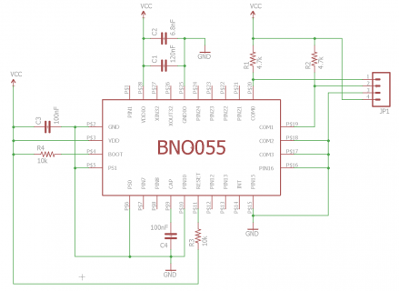
schematic.PNG

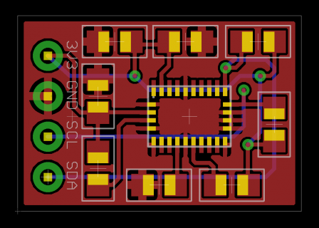
Board:
board.PNG

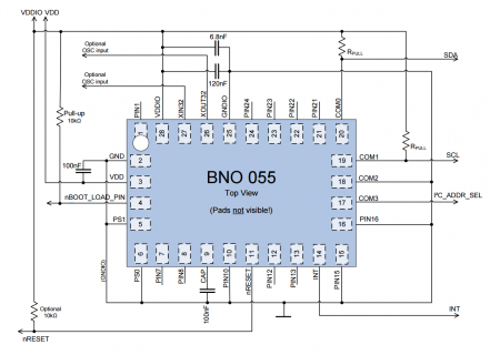
BNO055 Schematic:
BNO055-schematic.PNG

1) For the capacitors and resistors I'm using 0805 SMDs. I have some of the exact values that I need, but for some I do not and Digi-Key and Mouser only have them in reels of 3000 for the values I need. So for the 4.7k resistors, the closest I have is 4.3k and 5.1k. For the 6.8nF capacitor, the closest I have is 1nF and 10nF. And for the 120nF, the closest I have is 100nF. Can any of these be used instead of the actual values or do I have to find another way to get the exact value for them? For the 4.7k pull-ups, I imagine it's fine to use a close value, but for the capacitors I'm unsure.

2) I'm going to use OSH Park to have the boards fabricated, but I was also looking to get a stencil done since it would be hard to apply the solder paste by hand for the LGA BNO055. I found OSH Stencils (https://www.oshstencils.com/) by searching, which I don't believe has any affiliation with OSH Park, and was wondering if anyone has used them. If not, do you have any recommendations?

3) Is there anything about the board design in general that I should watch out for? Any issues with my board that I should fix before sending off the files?

Thanks in advance for all the help! I just download EAGLE CAD last week, and have been watching tons of videos and reading books on it so I still have a lot to learn.
 
Hi there, welcome to the world of PCB design.
Schematic looks fine to me. Only thing I might suggest is labelling pins on your header (JP1) in the schematic so you can be sure they're connected with the correct orientation (it can be very easy to flip a component over, rotate and hence pins be back-to-front if you follow me).
Those values you have should all be fine. The i2c pullups just dictate the current on the bus, 4.3k is well within 3mA spec. The 120nF and 6.8nF caps are decoupling caps; they help to smooth supply voltage out. 100nF and 10nF will be fine, although I'd argue perhaps the 10nF isn't necessary, based on the layout you've drawn. Where did the schematic come from you based it on?

I've not worked with Oshpark or Oshstencils before (from the UK so haven't used them).

One thing you don't have is component schematic numbers on your PCB, labelling, eg C1, R1 etc.

Other than that, on initial glance it looks good. Good luck!

Thanks for the advice Cosford! That's a good idea with labeling the pin header (I can see how easily it would be to get pins flipped/reversed). As far as the silkscreen for the components, I left those off since this is just for personal use and will just be soldering everything at home.

The BNO055 schematic shown is directly out of the datasheet (https://ae-bst.resource.bosch.com/media/products/dokumente/bno055/BST_BNO055_DS000_13.pdf) on page 97. That's great to hear about the resistor and capacitor values though...I sure didn't want to buy 3000 :)
 
I have had no trouble getting 120 nF and 6800 nF capacitors from Mouser in 0603 and 0402 sizes. I would recommend you use the values specified in the reference design. Make sure to size the voltage rating at 16 V or 25 V even better, this is because the capacitance droops at higher voltage and the charge pump on these chips might not have enough charge for correct operation if the voltage rating is too low. Make sure the power pins go to a bypass capacitor first and that the connection to the power rail is from the bypass capacitor (look like you have done). No topside copper under the package on any MEMS sensor! If you have a magnetometer, then no copper anywhere under the package.I don't care for component labels on my pcbs. It is enough to consult the schematic when assembling them to avoid mistakes unless you suffer from dyslexia.
 
I have had no trouble getting 120 nF and 6800 nF capacitors from Mouser in 0603 and 0402 sizes. I would recommend you use the values specified in the reference design. Make sure to size the voltage rating at 16 V or 25 V even better, this is because the capacitance droops at higher voltage and the charge pump on these chips might not have enough charge for correct operation if the voltage rating is too low.

Thanks Kris! I'll have to take a look online again...if they have them in the 0603 and 0402 sizes, I'm sure they do for 0805 as well (hopefully minimum quantity of 1).

Make sure the power pins go to a bypass capacitor first and that the connection to the power rail is from the bypass capacitor (look like you have done).

I studied your breakout board design over the past few days (https://www.tindie.com/products/onehorse/wearable-bno055-nano-board/), which helped tremendously. Thanks for making the files available on OSH!

No topside copper under the package on any MEMS sensor! If you have a magnetometer, then no copper anywhere under the package.

Wow, that's something I completely overlooked. You're absolutely right!
 
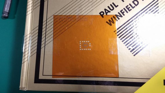
My stencil arrived today from OSH Stencils. I ordered it on October 19th (so it took 3 days total from the time I placed the order). The total was $7.86, including USPS First Class shipping which also includes tracking. The process was very easy, all I had to do was upload the board (*.brd) file from EAGLE. I'm impressed with how cheap it was, and how quickly it arrived.

Here are a few images of the stencil:

Full:
stencil-full.jpg

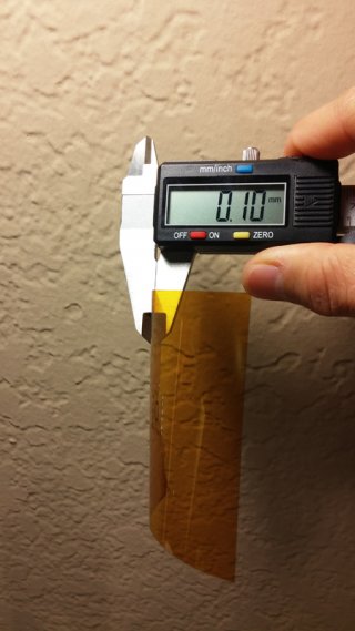
Thickness:
stencil-thickness.jpg

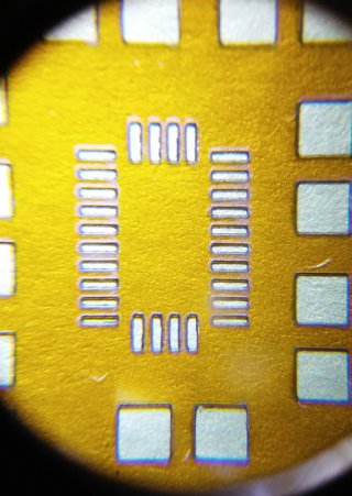
Magnified:
stencil-magnified.jpg

It is made from polyimide, and feels rather strong. I'm still waiting for the boards to arrive from OSH Park so I can't say how well the stencil works just yet. I'll likely just use the stencil for the LGA in the middle, and solder the 0805s by hand, but I'll still try to use the stencil for the entire board just to see how it does.
 
Hi there, welcome to the world of PCB design.
Schematic looks fine to me. Only thing I might suggest is labelling pins on your header (JP1) in the schematic so you can be sure they're connected with the correct orientation (it can be very easy to flip a component over, rotate and hence pins be back-to-front if you follow me).
Those values you have should all be fine. The i2c pullups just dictate the current on the bus, 4.3k is well within 3mA spec. The 120nF and 6.8nF caps are decoupling caps; they help to smooth supply voltage out. 100nF and 10nF will be fine, although I'd argue perhaps the 10nF isn't necessary, based on the layout you've drawn. Where did the schematic come from you based it on?

I've not worked with Oshpark or Oshstencils before (from the UK so haven't used them).

One thing you don't have is component schematic numbers on your PCB, labelling, eg C1, R1 etc.

Other than that, on initial glance it looks good. Good luck!

What is you suggestion for very small runs for which ospark is perfect pricewise, it's just slow in oversea shipment (to keep a affordable price).
Thanks.
 
A couple questions:

  • Where did you find the footprint spec? I searched everywhere but couldn't find it.
  • No crystal oscillator?
 
Consult the data sheet for the recommended land pattern (footprint). It is a straightforward design exercise. The crystal is only to reduce power usage, it is not really required nor does it affect accuracy (which is middlin') and makes it harder to realize a (n appallingly) small design.
 
Status
Not open for further replies.
Back
Top