Im posting this hear because I believe it may have a use to some who use Teensy's.
I have been researching 3d Printers for the past few weeks and I have seen several people use SSR's or standard relays to run the High Wattage Heat Beds and figured there should be a better way to drive a high power load with logic signals. Many 3d Printers are setup to drive 12Aish loads but anything more then that and bad things can/do happen. I have seen a few Mosfet Driver boards but none of them had Isolation on them. Which is something I like to use when driving large loads with micro's.
I figured since the printer kit I am looking at comes with a Relay and I plan to replace it ASAP I figured I would just create the board I wanted and give it enough functions to be useful for more then just 1 thing.
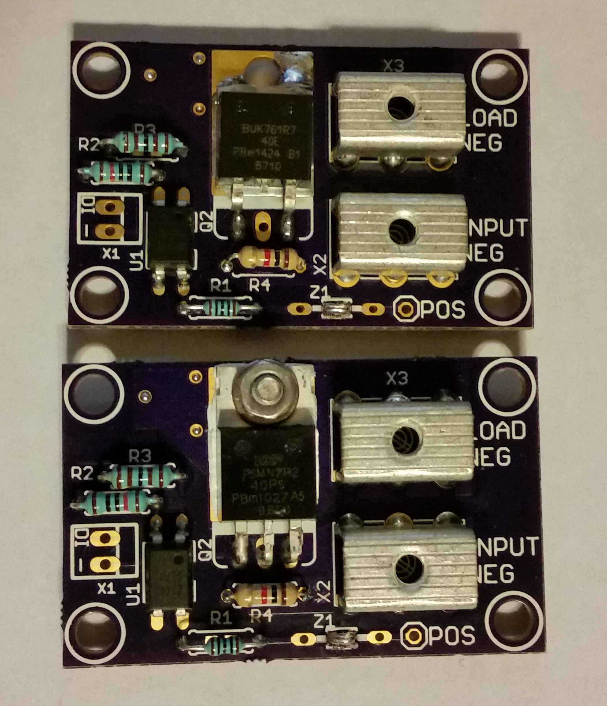
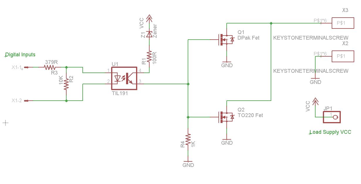
It uses cheap off the shelf Dip4 Opto Couples to drive low RDSon n-channel MOSFETs. This limits them to around 1Khz switching frequency.
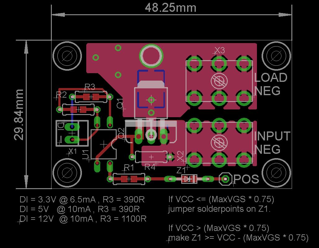
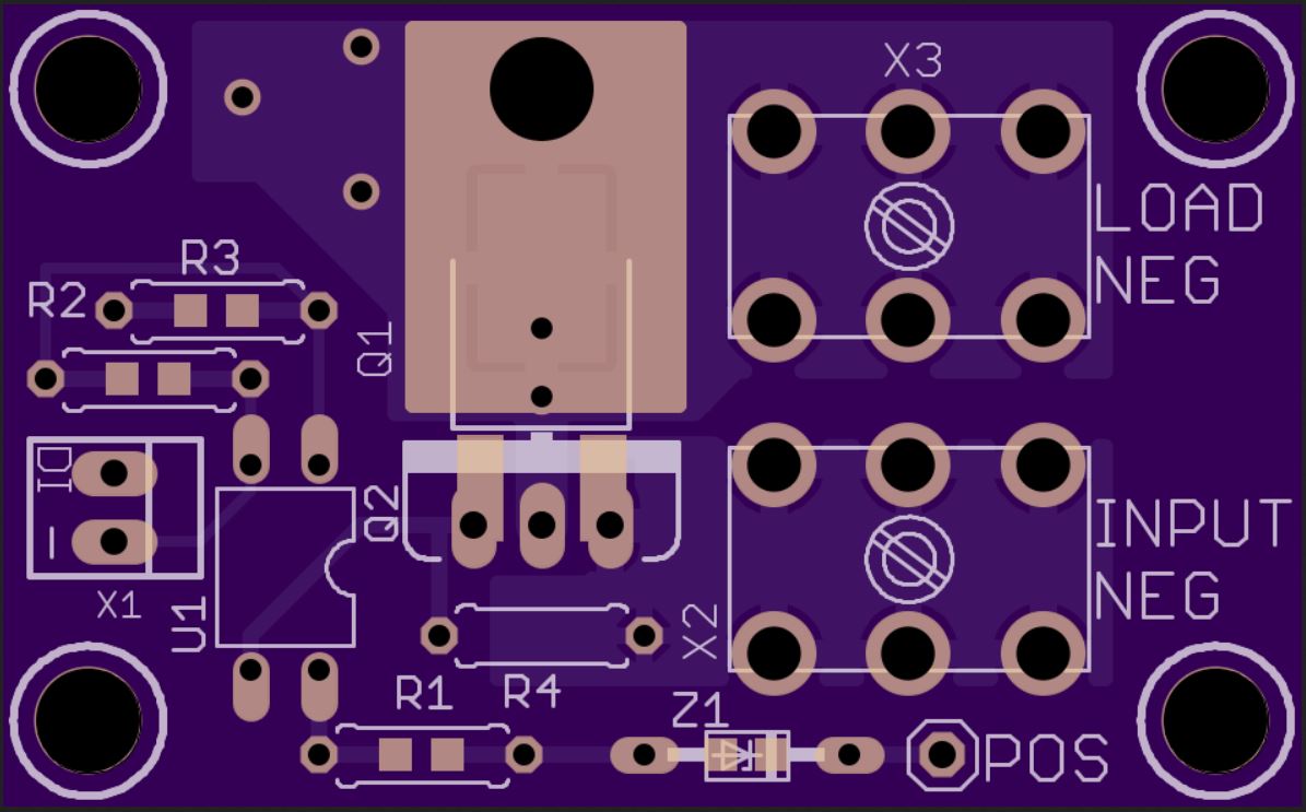
Its laid out to support either SMD or Thru-hole components(4pin SMD opto fits the Dip pads). The only exception is the 30A rated screw terminals for the load. The Pos supply and digital lines can be direct wired.
My goal is to be able to support up to 30A and up to possible over 100VDC(reason for Z1).
The basic Kit I might supply would be for a 12-24V Load and a 3.3-12V Digital input. The output limits would be specific to the Fet used and the amount of cooling.
I plan to build 3 prototypes with different setups, D2pak vs TO220 vs TO220+Heatsink to see what works and what does not work or at least where the limits need to be.
If those pan out as well as the simulations/math then I would make a larger kt batch based on interest/feedback.
Also.....
I have looked at making an even more powerful version for those insane 120VAC 600-1000W beds but the capacitors needed would almost quadruple the size of the board so I wont do it unless someone asks for it. The upside to it would be reduced current, the downside is 80-170VDC hurts")
I have been researching 3d Printers for the past few weeks and I have seen several people use SSR's or standard relays to run the High Wattage Heat Beds and figured there should be a better way to drive a high power load with logic signals. Many 3d Printers are setup to drive 12Aish loads but anything more then that and bad things can/do happen. I have seen a few Mosfet Driver boards but none of them had Isolation on them. Which is something I like to use when driving large loads with micro's.
I figured since the printer kit I am looking at comes with a Relay and I plan to replace it ASAP I figured I would just create the board I wanted and give it enough functions to be useful for more then just 1 thing.
It uses cheap off the shelf Dip4 Opto Couples to drive low RDSon n-channel MOSFETs. This limits them to around 1Khz switching frequency.
Its laid out to support either SMD or Thru-hole components(4pin SMD opto fits the Dip pads). The only exception is the 30A rated screw terminals for the load. The Pos supply and digital lines can be direct wired.
My goal is to be able to support up to 30A and up to possible over 100VDC(reason for Z1).
The basic Kit I might supply would be for a 12-24V Load and a 3.3-12V Digital input. The output limits would be specific to the Fet used and the amount of cooling.
I plan to build 3 prototypes with different setups, D2pak vs TO220 vs TO220+Heatsink to see what works and what does not work or at least where the limits need to be.
If those pan out as well as the simulations/math then I would make a larger kt batch based on interest/feedback.
Also.....
I have looked at making an even more powerful version for those insane 120VAC 600-1000W beds but the capacitors needed would almost quadruple the size of the board so I wont do it unless someone asks for it. The upside to it would be reduced current, the downside is 80-170VDC hurts
Last edited: