You are using an out of date browser. It may not display this or other websites correctly.
You should upgrade or use an alternative browser.
You should upgrade or use an alternative browser.
Test Points
- Thread starter loglow
- Start date
- Status
- Not open for further replies.
Thanks so much, that's perfect!
Constantin
Well-known member
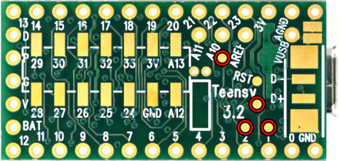
Same idea. The MKL02 bootloader likely gets programmed using those points.
That way, PJRC avoids having to unreel/program/re-reel MKL02 chips before sending them to the assembly fab for installation.
Instead, the fab sources 'virgin' MKL02's and reflows onto the board. After delivery to PJRC, Pauls bed of nails torture rig not only tests each board but also flashes the MKL02 chip.
Last edited:
Same idea. The MKL02 bootloader likely gets programmed using those points.
Cool, and thanks very much for that info.
When you say "same idea" do you mean that they're likely SWDIO and SWCLK (SWD interface) like on the Teensy 3.2? (the other T3.2 test points being USBID, RESET, and VDDA)
I don't know much about the SWD interface (or JTAG for that matter) and I didn't realize that it could be used to program chips like this. Can it?
Can anyone confirm or verify this? And also, which pin is which?
(I'm also assuming that T3.5/T3.6 schematics haven't been released yet, is that right?)
defragster
Senior Member+
I've not seen any schematics for either new Teensy yet, when I do they'll be linked on this K66 post
If you follow the traces on the pcb, they go to pin 14 and 16 from the KL02.
In the picture above:
left test point is pin 16/PTA2/SWD_DIO
right test point is pin 14/PTA0/SWD_CLK
If the KL02 chip is not write protected it can be programmed with the SWD interface. The KL02 chip stores the bootloader, if you program the KL02 with your own code, it'll destroy the bootloader function. It is not recommended to program the KL02 using the SWD interface.
Last edited:
PaulStoffregen
Well-known member
Indeed, don't mess with those test points. The protocol is very complex, so the odds of doing anything by mistake are slim. But if you do, the only likely outcome is bricking your Teensy. Don't do that.
If you follow the traces on the pcb, they go to pin 14 and 16 from the KL02.
In the picture above:
left test point is pin 16/PTA2/SWD_DIO
right test point is pin 14/PTA0/SWD_CLK
If the KL02 chip is not write protected it can be programmed with the SWD interface. The KL02 chip stores the bootloader, if you program the KL02 with your own code, it'll destroy the bootloader function. It is not recommended to program the KL02 using the SWD interface.
Thanks very much!
- Status
- Not open for further replies.


