K66 Beta Test

Status
Not open for further replies.
Oh, i completely missed that info.
This means someone could just edit the std sd - lib to use the SD-Slot with SPI ?
I'm could do that.. at least, we'd had a compatible way to use the inbuilt slot, then. preliminary .
FYI - I have played around with this, to be able to use the pins associated with the SDCARD for SPI pins, Uart pins, ...

I minor possible update to the core and SPI projects to allow this. I set it up to have those pins setup as pins 58-63:
My version of Core project with this is up at: https://github.com/KurtE/cores/tree/T35_USE_SDCARD_PINS it has a pull request that probably won't happen: https://github.com/PaulStoffregen/cores/pull/161

Likewise the SPI changes are at: https://github.com/KurtE/SPI/tree/T35_USE_SDCARD_PINS again pull request: https://github.com/PaulStoffregen/SPI/pull/19

The pin ALT table looks like:
Code:
58	PTE0	ADC1_SE4a	ADC1_SE4a	PTE0		SPI1_PCS1	UART1_TX	SDHC1_D1	TRACE_CLKOUT	I2C1_SDA	RTC_CLKOUT
59	PTE1	ADC1_SE5a	ADC1_SE5a	PTE1/LLWU_P0	SPI1_SOUT	UART1_RX	SDHC0_D0	TRACE_D3	I2C1_SCL	SPI1_SIN
60	PTE2	PTE2/LLWU_P1	ADC1_SE6a	PTE2/LLWU_P1	SPI1_SCK	UART1_CTS_b	SDHC0_DCLK	TRACE_D2		
61	PTE3	ADC1_SE7a	ADC1_SE7a	PTE3		SPI1_SIN	UART1_RTS_b	SDHC0_CMD	TRACE_D1			SPI1_SOUT
62	PTE4	DISABLED			PTE4/LLWU_P2	SPI1_PCS0	UART3_TX	SDHC0_D3	TRACE_D0		
63	PTE5	DISABLED			PTE5		SPI1_PCS2	UART3_RX	SDHC0_D2			FTM3_CH0
 
FYI - I have played around with this, to be able to use the pins associated with the SDCARD for SPI pins, Uart pins, ...

I minor possible update to the core and SPI projects to allow this. I set it up to have those pins setup as pins 58-63:
My version of Core project with this is up at: https://github.com/KurtE/cores/tree/T35_USE_SDCARD_PINS it has a pull request that probably won't happen: https://github.com/PaulStoffregen/cores/pull/161

Likewise the SPI changes are at: https://github.com/KurtE/SPI/tree/T35_USE_SDCARD_PINS again pull request: https://github.com/PaulStoffregen/SPI/pull/19

The pin ALT table looks like:
Code:
58    PTE0    ADC1_SE4a    ADC1_SE4a    PTE0        SPI1_PCS1    UART1_TX    SDHC1_D1    TRACE_CLKOUT    I2C1_SDA    RTC_CLKOUT
59    PTE1    ADC1_SE5a    ADC1_SE5a    PTE1/LLWU_P0    SPI1_SOUT    UART1_RX    SDHC0_D0    TRACE_D3    I2C1_SCL    SPI1_SIN
60    PTE2    PTE2/LLWU_P1    ADC1_SE6a    PTE2/LLWU_P1    SPI1_SCK    UART1_CTS_b    SDHC0_DCLK    TRACE_D2        
61    PTE3    ADC1_SE7a    ADC1_SE7a    PTE3        SPI1_SIN    UART1_RTS_b    SDHC0_CMD    TRACE_D1            SPI1_SOUT
62    PTE4    DISABLED            PTE4/LLWU_P2    SPI1_PCS0    UART3_TX    SDHC0_D3    TRACE_D0        
63    PTE5    DISABLED            PTE5        SPI1_PCS2    UART3_RX    SDHC0_D2            FTM3_CH0
Great !
Half an hour ago, i began working on this, and noticed that some work has to be done for these pins..
Now, i saw your post :)
Thank you.
I added a notice for Paul @ github.
 
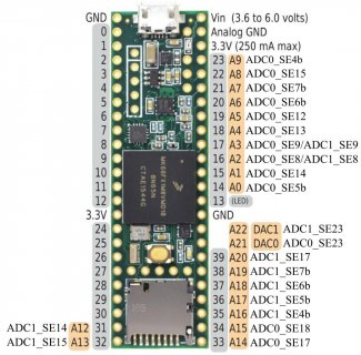
Here a draft of the latest pinout card. Hopefully I got all the pins right this time?

View attachment 7968

I should explain a sort of double standard regarding display of alternate pin functions. For communication signals, alternates are shown. But for PWM and SPI chip selects, alternate locations are not shown on the pinout card. For example, pin 25 is PTA5 & FTM0_CH2, but it's not shown as PWM because we use pin 9 for that FTM0_CH2 signal.

do you have the back side pinout?
 
Here a draft of the latest pinout card. Hopefully I got all the pins right this time?

View attachment 7968

I should explain a sort of double standard regarding display of alternate pin functions. For communication signals, alternates are shown. But for PWM and SPI chip selects, alternate locations are not shown on the pinout card. For example, pin 25 is PTA5 & FTM0_CH2, but it's not shown as PWM because we use pin 9 for that FTM0_CH2 signal.

Looks pretty good, I noticed a few PWM's that are missing, that or I misread the datasheet(would not be the first time).

PWM's on: 13(PTC3, FTM0_CH2), 25(PTA5, FTM0_CH2)
 
Looks pretty good, I noticed a few PWM's that are missing, that or I misread the datasheet(would not be the first time).

PWM's on: 13(PTC3, FTM0_CH2), 25(PTA5, FTM0_CH2)

Actually this is the case Paul mentioned in the stuff you quoted:
I should explain a sort of double standard regarding display of alternate pin functions. For communication signals, alternates are shown. But for PWM and SPI chip selects, alternate locations are not shown on the pinout card. For example, pin 25 is PTA5 & FTM0_CH2, but it's not shown as PWM because we use pin 9 for that FTM0_CH2 signal.

That is a program can only use one physical pin corresponding to a timers channel, in this case FTM0 channel 2, and for the default Paul choose Pin 9 for it. As I mentioned for CS pins, it would be nice if there was a more detailed card or the like, could potentially put on main card with maybe with gray text, maybe show a number next it, could be some form of channel number or the pin it is duplicate of... But again I understand only so much space and it could soon become confusing.
 
Unused Interrupt channels

Some time ago, there was a discussion to use unused IRQ channels for software interrupts.
For the T3.2 it turned out that there are plenty of them.
For the T3.6 there are only 4 {46,71,84,85}, not counting IRQ_SOFTWARE
where only 71 is common with T3.2

I have not checked if there are more possible (due to unused HW pins), but these four have no assigned functionality.
 
You can use any other too, as long the original functionality is not needed.

I updated the MP3/AAC-Codecs to use 71, some time ago.

Edit:
Perhaps it's time now to add some #defines for unused interrupts to the core ?
 
Last edited:
You can use any other too, as long the original functionality is not needed.

I updated the MP3/AAC-Codecs to use 71, some time ago.

Edit:
Perhaps it's time now to add some #defines for unused interrupts to the core ?

Maybe also indicating interrupts that by hardware design are excluded from being useful
 
Paul - I put the updated rev of the Teensy™ 3.6 card on post 8 with a link to that post.

Don't forget Teensy™ - or whatever you need to use. Teensy™ might be good to note in a KS Update as well to make it public record. Maybe even update the KS Campaign page.

Also I noted about exposed DEBUG pins on the @MM Why Teensy™ 3.5 or 3.6? thread that other than answering a comment, debug pin exposure isn't listed as a common K66/K64 board feature.
 
Borrowed Pauls card from post #1245 and added the ADC's to it.
Teensy_card9a_rev1_Analogs.jpg

@Paul, looking at the datasheet it says the DAC's have access to two references. Are the two available references tied together or can they be fed an external reference?
Also do you know when you will have a backside Teensy3.6 card ready for us to hack-up:cool:?

41.1.3 12-bit DAC Reference
For this device VREF_OUT and VDDA are selectable as the DAC reference.

VREF_OUT is connected to the DACREF_1 input and VDDA is connected to the
DACREF_2 input. Use DACx_C0[DACRFS] control bit to select between these two options.

Be aware that if the DAC and ADC use the VREF_OUT reference simultaneously, some
degradation of ADC accuracy is to be expected due to DAC switching.


At some point I need to clean up my Eagle Symbol and I do have a Kicad Symbol/Footprint I just need to clean them up and do similar repairs to the Symbol.
 
Hi all, just wanted to let people know I have a new Version(6) of Snooze that supports Teensy 3.5 and I just fixed a bunch Teensy LC issues also. It has a few api changes but very similar to the old version 5. All the examples show this and should not be to much to change existing code. There are also a bunch of upgrades that I hope make it conflict less with other libraries or user code. One such upgrade it that it saves pin state before going to sleep and restores it back after waking up. So for an example if you want to use Serial1 RX pin as a wakeup pin and still have Hardware Serial1 work after sleeping it should work without having to configure anything. This is still beta but I want to put it out now so I can get some fresh eyes on it to see what other bugs or short comings there are before merging it to Version 5.

tried snooze v6 on T3.6 (K66) (IDE 1.6.11 1.30-beta3). sleep example flashes every 10s, and digital pin wakeup ok,though I'm not sure how to get touch to work?? measuring 1.4 ma

(v6 sleep example won't compile on T3.5(K64), no touch pins on K64, and there may be other mods needed for K64?)
 
Last edited:
Quick update, on I2C I was able to get all four buses to talk to each other on K66. Wire as a master device, and the other three as slaves (had to use the 10-pin header location to get Wire3, as per post #8 info). Everything works correctly. That was done using external pullups.

So then I got to wondering about internal pullups, so I tried configuring it for that. I knew something was probably not going to work when I saw the pin LEDs double in brightness when I went from external pullups to internal. Sure enough, I couldn't get loopback to work with internal pullups.

So I figured I would measure the resistance. Well I thought Freescale really botched the T3.1/3.2 pullups when they measured out at <200 ohms, but that's got nothing on the T3.6 which I measured at ... 24 ohms. :p

Now it's possible I got the wrong internal pin config, so I'll go check the port configs again to see if bits shifted or something, but if someone could verify this number that would be helpful. Note that pullup strength when I2C is active vs not active, is not the same, the pin must be configured for the correct I2C ALT setting. IIRC normal pin pullups are generally reasonable.

I measured I2C internal pullup (pins 18 19) on K66 at 17 ohms (using 470 ohm as voltage divider). For K64, I measured 150 ohms
 
Hi Paul,

Front side looks good.
Took a quick look through the backside and everything looks good to me. Note: Pin 55 is also a CS2, but duplicate of 43...

The only things I don't see documented here are the D+ and D-, which on the T3.2 card you show as USB Signals. And likewise the H and D pads, which I believe are used in the USB Host Port for Host versus Device...

Hopefully in the production version of boards, there will be something to help make it more obvious is it a 3.5 or 3.6, other than looking very closely to see MK66 or MK64 and a couple of missing small parts near USB host pins. Like a stamp, or some color dot or ??? If so maybe good to mention or show the difference on card?
 
Is it possible to use a different color for the arrow to the interior pins ? It is not good visible.
Good point Frank.

From the back of the Teeny_LC card::
Teensy-LC pins are not 5 volt tolerant. Do not apply more than 3.3V.

Perhaps a HOLOGRAPHIC printed card that shows alternate pin functions at different angles?
 
The only things I don't see documented here are the D+ and D-, which on the T3.2 card you show as USB Signals. And likewise the H and D pads, which I believe are used in the USB Host Port for Host versus Device...

Yeah, I'll try to cram those in. At least there's a small amount of space remaining on the back side.

Hopefully in the production version of boards, there will be something to help make it more obvious is it a 3.5 or 3.6,

Well, there is the big title at the "Welcome to Teensy 3.6" and "Teensy 3.6 Back Side". ;)

As I mentioned in another post, none of the pinout cards list the i2s pins.

Yeah, I've never put the I2S pins on the cards, partly due to limited space, partly in the interest of keeping the card simpler and easier to use, and partly based on the assumption most use cases for those signals will involve a shield.

Likewise for the ethernet pins on these new boards.

It sure would be great to have which pins (channels) work with which timers documented on that card.

Who does that really help?

The cards are meant to be a quick reference for the most commonly needed signals. There just isn't enough room to show all pin info. The idea is to help people plugging wires into breadboards and hand soldering prototype have something small and simple right next to where they're doing the work. It greatly improves the chances of getting the wires connected correctly, compared to looking back and forth to a PDF over on a computer screen.
 
Hopefully in the production version of boards, there will be something to help make it more obvious is it a 3.5 or 3.6, other than looking very closely to see MK66 or MK64 and a couple of missing small parts near USB host pins. Like a stamp, or some color dot or ??? If so maybe good to mention or show the difference on card?

Paul - as I read this it was saying the PCB (which of course is COMMON) gives no OVERT indication to what you are holding in your hand?

... as asking for a clear note on the card that says: If this space is "empty it is a T_3.5", if it is "populated this is a T_3.6".

And as noted before if there were a sticker or some color specific INK BLOB/Stamp applied. Perhaps boards that pass the AUTO POGO TESTER would get a WHITE "T_3.5 QC" passed stamp applied (on the open bottom area under the MCU?) and then a clearly different verbiage or color stamp indicating "T_3.6 QC" passed like I see on other motherboards? Obviously the silk screen can't handle this - but post production could.
 
Fair enough. I can say that I feel more information about Timers and PWM should be provided somewhere more central (perhaps as one of the example sketches). I spent more thrash time than I feel I should have puzzling over and eventually figuring out why I couldn't have different PWM values in different pins due to the way the pins related to the timers on the backend.
 
Well, there is the big title at the "Welcome to Teensy 3.6" and "Teensy 3.6 Back Side". ;)
As Defragster mentioned, it was more of a question of if I have 4 of these chips sitting on my desk and some are 3.5s and others are 3.6s how do i quickly recognize which ones are which.

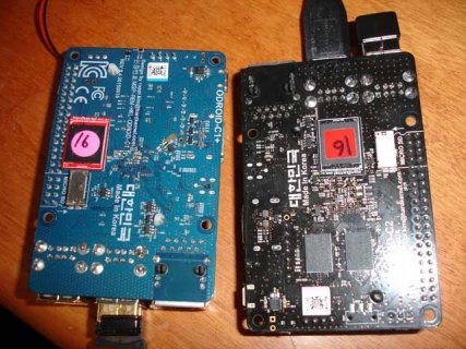
As Defragster mentioned, you could put a sticker or different color dot on one or both of them. Example for my Odroids, they have eMMc chips that can use (or you can use SDCard). All of the chips look pretty much the same, so you need to know which ones work with different boards.

Here is a picture of a C2 and C1+
Odroids.jpg
The small things with 16 on them are the emmc chips that connect through a small connector. In this case the chips are different colors as well, but many times they are the same color and so they used different color dots... But my guess is that you can do something a little less obtrusive, like maybe one of them has a simple red dot (paint?) on the chip?

Kurt
 
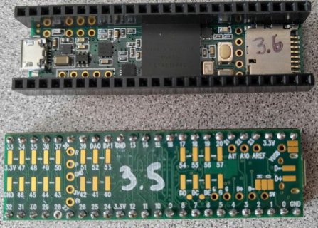
Also "Teensy" on these newest cards might be marked as 'Trademark'.

Hold down the ALT key and on your numeric keypad, enter the number 0174 for ® or 0153 for ™

marked_K66K64.jpg
 
Last edited:
Status
Not open for further replies.
Back
Top