
You are using an out of date browser. It may not display this or other websites correctly.
You should upgrade or use an alternative browser.
You should upgrade or use an alternative browser.
Teensy CC Dummy Load +300W
- Thread starter Donziboy2
- Start date
- Status
- Not open for further replies.
Think i'm going to change my dividers for the DACs and the current measurements from 14K and 10K7 to 14K7 and 10K2. It would drop my max current from 21.66A with a resolution of 1.0578715mA to a max current of 20.482A with a resolution of 1.0003383mA. I think that's the closest to 1ma per bit I can get without adding more resistors.
I also need to look into how the DAC's are initialized, I read a comment from Paul on another thread that said they would go to around 1.65V when initialized. If that is the case I will need to add a pull down fet/bjt at the input to prevent the Load Fets from firing by mistake during startup or restart due to loss of power.
If it rains this weekend I will work on the Dummy load prototype, if not I will play around with my E-gocart.
Last edited:
Futzed around with changing the above mentioned resistors and decide against it, I would not really gain much of anything and would loose headroom that may be needed depending on how much sag the 3v3 rail has.
Played around with changing the sense resistors to 3 or 5W resistors, not sure I like it. The reduced resistance posses some issues of noise and sensing.
Currently I have a 0.33 ohm sense resistor, meaning at 12bit I have a resolution of roughly 35uV per bit at the resistor. If I reduce the resistance to say 0.1 ohm, I would have a resolution of 10.6uV per bit at the resistor. Now if Opamps where perfect it would not matter but sadly they aren't. Add noise and natural offsets to the mix and it just gets ugly.
Started reworking the board. Think im going to go to a 150mm x 150mm board from 150x100. I want better spacing between some components and the addition of the Teensy 3.6 took almost a square inch of what little space I had to begin with away.
Started playing around with a 20X4 LCD, it will be the most basic screen so I figured I would start there and get an idea of what I will be able to do without getting in the way of my ADC's.
The below code along with an O-scope gave me some info, I also tried a few more combinations of the below commands to see what happens.
Writing all 80 characters takes roughly 2.87mS.
Writing 40 characters takes 1.444mS.
Writing 30 characters takes 1.102mS.
Writing 20 characters in the first line takes 662uS.
Writing 5 characters in the first line takes 143.2uS.
Sending the Clear or Cursor command and moving on only takes 10-14uS sometimes, other times it takes 40ish uS to do a cursor change.
Cursor changes from row 0 to 2, 2 to 1 and 1 to 3 took just under 40uS each.
Cursor changes from row 0 to 1 and 2 to 3 took roughly 14uS but 1 to 2 took roughly 40uS.
If you do a Clear and a Cursor command it takes much longer. Most likely you have to wait to clear the screen then you can send the Cursor command.
Clearing and setting the cursor on a screen with 20 characters displayed takes 640ish uS.
Clearing and setting the cursor on a screen with 21 or 80 characters displayed takes 1.43ish mS, same for 40 characters.
Code:
#include <LiquidCrystalFast.h>

const int pulse = 14;
const int tick = 16;

// initialize the library with the numbers of the interface pins
LiquidCrystalFast lcd(12, 10, 11, 5, 4, 3, 2);
         // LCD pins: RS  RW  EN  D4 D5 D6 D7


elapsedMillis startloop;
      byte teststate = 0;

void setup() {


  pinMode(pulse, OUTPUT);
  pinMode(tick, OUTPUT);


  // set up the LCD's number of rows and columns:
  lcd.begin(20, 4);
  // Print a message to the LCD.
  lcd.print("hello, world!");

  delay(10000);
startloop = 0;
}

void loop() {
// as long as pulse is pulsing the loop is not being blocked
digitalWriteFast(pulse, HIGH);
digitalWriteFast(pulse, LOW);

  if (startloop >= 100  && teststate == 0){     //test Clear
    digitalWriteFast(tick, HIGH);
    lcd.clear();
    teststate = 1;
  }
  if (startloop >= 200 && teststate == 1){      //Set cursor
   digitalWriteFast(tick, LOW);
   lcd.setCursor(0,0);
   teststate = 2;
  }
  if (startloop >= 300 && teststate == 2){      //Write A
   digitalWriteFast(tick, HIGH);
   lcd.print("A");
   teststate = 3;
  }
  if (startloop >= 400 && teststate == 3){      //Clear A
   digitalWriteFast(tick, LOW);
   lcd.clear();
   teststate = 4;
  }
  if (startloop >= 500 && teststate == 4){      //Reset Cursor
   digitalWriteFast(tick, HIGH);
   lcd.setCursor(0,0);
   teststate = 5;
  }
  if (startloop >= 600 && teststate == 5){      //Write 1
   digitalWriteFast(tick, LOW);
   lcd.print("1");
   teststate = 6;
  }
  if (startloop >= 700 && teststate == 6){      //Reset Cursor
   digitalWriteFast(tick, HIGH);
   lcd.setCursor(0,0);
   teststate = 7;
  }
  if (startloop >= 800 && teststate == 7){      //Write 20 Chars
   digitalWriteFast(tick, LOW);
   lcd.print("Fortheloveofspeeding");
   teststate = 8;
  }
  if (startloop >= 900 && teststate == 8){     //Clear and set cursor
   digitalWriteFast(tick, HIGH);
   lcd.clear();
   lcd.setCursor(0,0);
   teststate = 9;
  }
  if (startloop >= 1000 && teststate == 9){    //Fill the entire screen
   digitalWriteFast(tick, LOW);
   lcd.print("ABCDEFGHIJKLMNOPQRSTUVWXYZabcdefghijklmnopqrstuvwxyz0123456789!@#$%^&*0123456789");
   teststate = 10;
  }

  if (startloop >= 5000 && teststate == 10){   //Long Pause
    teststate = 0;
    startloop = 0;
  }
}Yep i'm still working on it here and there. I just ordered parts to build a sepic test board for the power supply. I have also been playing around with replacing the +-12V supply with a linear regulator set to 10V and a charge pump for -5V.
Its one of a few projects im playing with.
Its one of a few projects im playing with.
For higher resolution, you can go to 13bit from the 12bit I have listed. Each of my channels can read up to roughly 4.332A(1.0579mA/bit), if you reduce it to just above 2A you can increase the resolution again.
Just the 2 above changes would give you a factor of 4 increase in resolution over what I have proposed. You would have about +/-250uA per bit at 13 bit resolution.
You may be able to squeeze one more bit out of it if you sample the crap out of the ADC and then average it.
If you want more resolution then that you either need to invest in external ADC with good reference or you could split the load up with more Fets.
For higher resolution, you can go to 13bit from the 12bit I have listed. Each of my channels can read up to roughly 4.332A(1.0579mA/bit), if you reduce it to just above 2A you can increase the resolution again.
Just the 2 above changes would give you a factor of 4 increase in resolution over what I have proposed. You would have about +/-250uA per bit at 13 bit resolution.
You may be able to squeeze one more bit out of it if you sample the crap out of the ADC and then average it.
If you want more resolution then that you either need to invest in external ADC with good reference or you could split the load up with more Fets.
Good things to ponder. I will post here with ideas...
So I decided to remove the DC-DC iso supply I was using for +12/-12V for the Opamps.
Couple of reasons.
1. Cost, the Dc-Dc Iso supply was $6 vs about $3 for the Linear supply(LM317) and charge pump(LM2776), including caps and resistors.
2. Increased output capability. Both the LM317 and LM2776 can output more current then the DC-DC Iso supply's could ever produce.
3. We don't actually need +12v or -12V, we can get away with a much lower negative voltage since its there to ensure the OpAmp's can get to at least 0V on the gates. We also don't need +12V since the majority of Fet's we would use turn on much sooner and we are trying to drive them linearly so we should in theory never need more then 6-7V.
So I decided to remove the DC-DC iso supply I was using for +12/-12V for the Opamps.
Couple of reasons.
1. Cost, the Dc-Dc Iso supply was $6 vs about $3 for the Linear supply(LM317) and charge pump(LM2776), including caps and resistors.
2. Increased output capability. Both the LM317 and LM2776 can output more current then the DC-DC Iso supply's could ever produce.
3. We don't actually need +12v or -12V, we can get away with a much lower negative voltage since its there to ensure the OpAmp's can get to at least 0V on the gates. We also don't need +12V since the majority of Fet's we would use turn on much sooner and we are trying to drive them linearly so we should in theory never need more then 6-7V.
View attachment 8712
The thing is that the LM2776 produces a crazy amount of output ripple (>100mV for small currents). For this reason, I am not a big fan of it in combination with a linear voltage regulator (like the LM317), which has very low ripple.
I would rather use an LTC1550 which, although not being able to source as much current as the LM2776 and costs $2 instead of $1, can still go up to 50 mA (at a 6.5V VCC) and has ripple characteristics <=1mV. Since a lot of current is not needed for op-amp use, this may be a better solution if ripple characteristics are important (i.e., depending on the PSRR of the op-amps employed).
Last edited:
Updated the first page with latest schematic. I got rid of the 4x20 LCD and am going to use the ILI9341 with Frank B's DMA library.
I also got the T3.6 on the page and have started figuring out what pins will go where. There is also an output (Lockout) that will hold the Op Amp inputs at 0V until I am ready to enable the system.
The Sepic prototype should arrive next week. I can start load testing it to get an idea of what input voltage's will work for this application along with max load current.
The thing is that the LM2776 produces a crazy amount of output ripple (>100mV for small currents). For this reason, I am not a big fan of it in combination with a linear voltage regulator (like the LM317), which has very low ripple.
I would rather use an LTC1550 which, although not being able to source as much current as the LM2776 and costs $2 instead of $1, can still go up to 50 mA (at a 6.5V VCC) and has ripple characteristics <=1mV. Since a lot of current is not needed for op-amp use, this may be a better solution if ripple characteristics are important (i.e., depending on the PSRR of the op-amps employed).
Looking at the example circuit for the LTC1550 I see why it has such low ripple. It only uses 0.1uF charge caps and it uses larger output caps, they dont jump out and say it but im sure its impedance is pretty high. Edit, its also a regulated charge pump vs unregulated. I would only be feeding 5V so I would be limited to 20mA. Not sure I want such a low amount of current. Driving 4 Op Amps and 5 fets.
I will look further, I had not noticed the high ripple at low loads on the LM2776, I will look at other options or adding extra filtering.
Last edited:
Think I will need to rethink the Sepic. Testing with minimum 4.5V input and 12.3V out @ 300mA seems to be the safe limit for my test setup. I attempted to raise the limit to 370mA(at 4.5 and 5V input) after letting it soak at 300mA for a while and it ran for about a minute before the Sepic shut itself down.
The inductor I chose was overrated by about 250% so I could see if I can find a bigger sepic IC that can do 2-3A. The LT1961 is only rated at 1.5A.
I need to get more of the parts together and measure the actual load needed to keep it all running. I was guessing at around 350mA, which is to close to the apparent limit of this design. The other factor is, what are the chances someone wants to run this with a 5v 2A USB Battery other then myself?
Did some measurements with a T3.1 DAC dis-morning(I will retest with a 3.6 when its done on another project). Found that it can pull a 20K resistor down to 10mV roughly, with about 20mV of noise. I added a 5Meg pull down to -4V and added a 10pF cap to reduce noise. The 5Meg pulls the 10mV signal when the DAC is set low to -3mV, allowing me to turn the current down in much finer steps at the low end, the upper limit was not affected much since I assume anything past 3.2V from the DAC is extra headroom(T3.1 DAC made it to roughly 3.29V).

I also made changes to the Output lockout so that it would actually do what it is supposed to do, force the outputs off during startup or when the system is not enabled.

I also made adjustments to the resistors on the LEDs to reduce current consumption to roughly 1mA each. I increased the resistor going to the LCD Back-light from 100R to 33R, its probably overkill indoors but its adjustable.
Still not sure if I should stick with the LT1961. I can either raise the minimum voltage meaning 5V input would not be feasible, find ways to reduce current draw, go with a different Sepic IC, or drop the idea of using a Sepic and use a different scheme.
Newest schematic is up on first page.
I also made changes to the Output lockout so that it would actually do what it is supposed to do, force the outputs off during startup or when the system is not enabled.
I also made adjustments to the resistors on the LEDs to reduce current consumption to roughly 1mA each. I increased the resistor going to the LCD Back-light from 100R to 33R, its probably overkill indoors but its adjustable.
Still not sure if I should stick with the LT1961. I can either raise the minimum voltage meaning 5V input would not be feasible, find ways to reduce current draw, go with a different Sepic IC, or drop the idea of using a Sepic and use a different scheme.
Newest schematic is up on first page.
Had some free time so worked on the PCB, I still need to do testing of some of the circuits. But I have a pretty good idea of what it will look like now

Still have some cleanup to do but I think its a decent start, I need to order some parts in the next few days to test parts of the circuit(supplies) that I need to confirm before I commit to them, I should also have some ILI9341 Touch screens coming from PJRC in the next few days to test power requirements.
Still have some cleanup to do but I think its a decent start, I need to order some parts in the next few days to test parts of the circuit(supplies) that I need to confirm before I commit to them, I should also have some ILI9341 Touch screens coming from PJRC in the next few days to test power requirements.
Last edited:
Performed a few more tests on the LT1961, it looks like going over 300mA@12V output with it would not be wise with a 4.5V input. The 2 bottom rows in red where unsustainable for more then a few minutes, it has been running happily for over an hour at 302mA but going over seems to rub it the wrong way and it heats up quickly and shuts down. Granted the PCB is only 1.26 square inches, I think pushing it harder would just cause issues.

I have been looking at 2 IC's from TI that would do the job, they are pin compatible with each other, they also have adjustable frequencies. The TPS61175PWPR and the TPS55340PWPR .
The 61175 is rated at 3A with a 18V max input and 38V max output. 5 cents more then the LT1961
The 55340 is rated at 5.25A with a 32V max input and 38V max output. $1.16 more then the LT1961
For the vast majority of people I think the 61175 would work, the 55340 would only be needed if you wanted 24V input capability.
Learned a few new things and had to put on my dunce cap for a few minutes today.
The ILI9341 Touch Screens PJRC sells (TJCTM24028-SPI) have a small 3R9 resistor in series with the back light LED. Meaning you can apply 3.3V directly to the LED pin and you will get about 48mA of draw from the back light.
The dunce cap was required when I tried to set up the PWM circuit for the LED back light and I used an NMOS.... I then spent about 10 minutes trying to figure out why I was only getting 2.8mA into the LED's instead of the 48mA I was expecting.
I went ahead and swapped the LT1961 with the TPS55340/61175.
As usual the first page has been updated with the latest schematic.
My battles continue, today I attempted to test an LM2776 only to find it is very hard to bread board them due to there sensitivity to inductance of traces and long leads. Short of creating a small pcb just for testing it I may be SOL. I am contemplating dropping it for a Murata DC-DC Isolated 5V 1W supply CRE1S0505SC.
In other news I successfully installed a temporary display on my E-Go Cart, and then a few minutes later blew one of the 168A Mosfets just sitting in my shed moving it back and forth a few feet.....
Edit....
Did a little more reading on the CRE1S0505S3C, with a 10%(minimum required for spec) load and a small inductor at the output I can achieve 5mV p-p.
edit 2
Adding the inductor to the CRE1S0505S3C wont work, its for a different model with much higher ripple. CRE1S0505S3C spec at 15mV typical and 25 Max.
Last edited:
Perhaps a stupid question:
In reviewing multiple electronic load designs, including yours, it seems like they are all designed to effectively place a short on the power supply being tested with the load (well not exactly a dead short, but whatever the Rds resistance of the MOSFET(s) happens to be). This is because the MOSFETs are effectively being used as on/off switches to either "short" the supply or not. To make the resistance of the MOSFETs variable, they would have to be run in their linear regions, but in these regions it seems like one has poor control over the (value of the) current going through the MOSFET, especially for small currents in the mA.
So let me ask the question that I am trying to figure out: Does this load design allow one to actually control the current being placed on the supply under test by being able to vary the resistance of the load? In other words, what if I want to test with a 1 A load or a 100 mA load, can I select that, given a particular input voltage being placed across the load by my supply?
Last edited:
Most commercial electronic loads do this, and is considered the pro forma design. Easier to do microprocessor-controlled loads using voltage device rather than a current device (bipolar transistor).
Recently did a quicky proto for a harmonic load for the factory. Used three T3.2 and three banks of FETs. This design will be formalized and be made pretty to enable my employer to submit data to UL for k-factor rating for a 600kVA transformer. Gate capacitance and drive signal integrity become very important design factors for this type of stuff.
Recently did a quicky proto for a harmonic load for the factory. Used three T3.2 and three banks of FETs. This design will be formalized and be made pretty to enable my employer to submit data to UL for k-factor rating for a 600kVA transformer. Gate capacitance and drive signal integrity become very important design factors for this type of stuff.
Not sure how much more I will put into this, at some point I will just bite the bullet and get boards made. Dont I found some mistakes


Latest Schematic 12-11-16
The only items I have doubts about are:
1. The LCD will need 4-8 inches of wire to reach the board. Im not sure how badly it would affect the SPI.
2. If I installing the LM4040-2.048V reference and change the sense resistors to 0.25R. The op-amp gains would need adjustment but I would get signals very close to 1mA/Bit at 12Bit resolution. The max theoretical current would be 20.48A.
Last edited:
Still working on this when not playing with my electric Gocart, did some optimizations with the resistor values, removed a few values that I could get away with and removed the extra fan hardware.
Recalculated the Vinput divider.
Recalculated the DAC dividers.
Recalculated the Temperature sensors.
Recalculated the LED Current.
The 2.048V reference is now required.
Got ride of the dividers for the Iout readings.
Added Piezo output.
Fan hardware is now PWM driven standard for PC fans. Removed the extra bits and pieces to this, PWM fans are so easy to get nowadays.
I have also been poking around the power supply side. I found Pololu carries a sepic power supply and it uses the same TPS55340 I was planning to use. I'm going to order 1 and see how well it works.
The connections to the Teensy are still not set completely, I still have things I need to check before I consider them final. I have not had time to look at the display requirements in depth, or test any code other then some playing with ADC DMA and the DACs.
I would like to have SD card logging at a minimum and maybe some wired/wireless comms. Not sure what pins I would want, the number of available pins on the Teensy 3.6 is pretty low also:/. I know sending with the USB on the Teensy has some delay and it can actually cause timing issues if the PC takes to long so I want to avoid that.
I'm also looking at increasing the PCB size from 150x100mm to 150x150mm. I would like to space some items out a little more then they are and I have run out of room using the 150x100mm size.
Latest Schematic
WIP Cad Rendering (PCB holes are out of place, its an old IDF)
Still tinkering, mostly in Kicad/Autocad, I need to get going on the screen at some point. I came across Scullcom Hobby Electronics on Youtube and have been watching many of his videos. I'm currently looking at making a Millivolt meter based on Barbouri's take of Scullcom's design. And most likely a Voltage reference board.
Recalculated the Temperature sensors again, went wrong way first time and made resolution worse.
The external reference is now an MAX6070AAUT21. Its a 2.048V reference with 0.04% accuracy and a Temp Co of 6ppm/C. It does require removing the 470R from the Teensy but that's not to difficult.
Recalculated the Temperature sensors again, went wrong way first time and made resolution worse.
The external reference is now an MAX6070AAUT21. Its a 2.048V reference with 0.04% accuracy and a Temp Co of 6ppm/C. It does require removing the 470R from the Teensy but that's not to difficult.
Made a few more changes, added a supervisor IC to keep the Teensy from having startup issues that have plagued other users. Updated Schematic on first page.
Removed resistor from FAN-PWM, found it was not needed. Also found that even pulling FAN-PWM low will not fully turn off the fans. May have to add an off circuit if I want to turn it off.
Going to try to space some of the stuff out, its pretty tightly packed together and I have room.
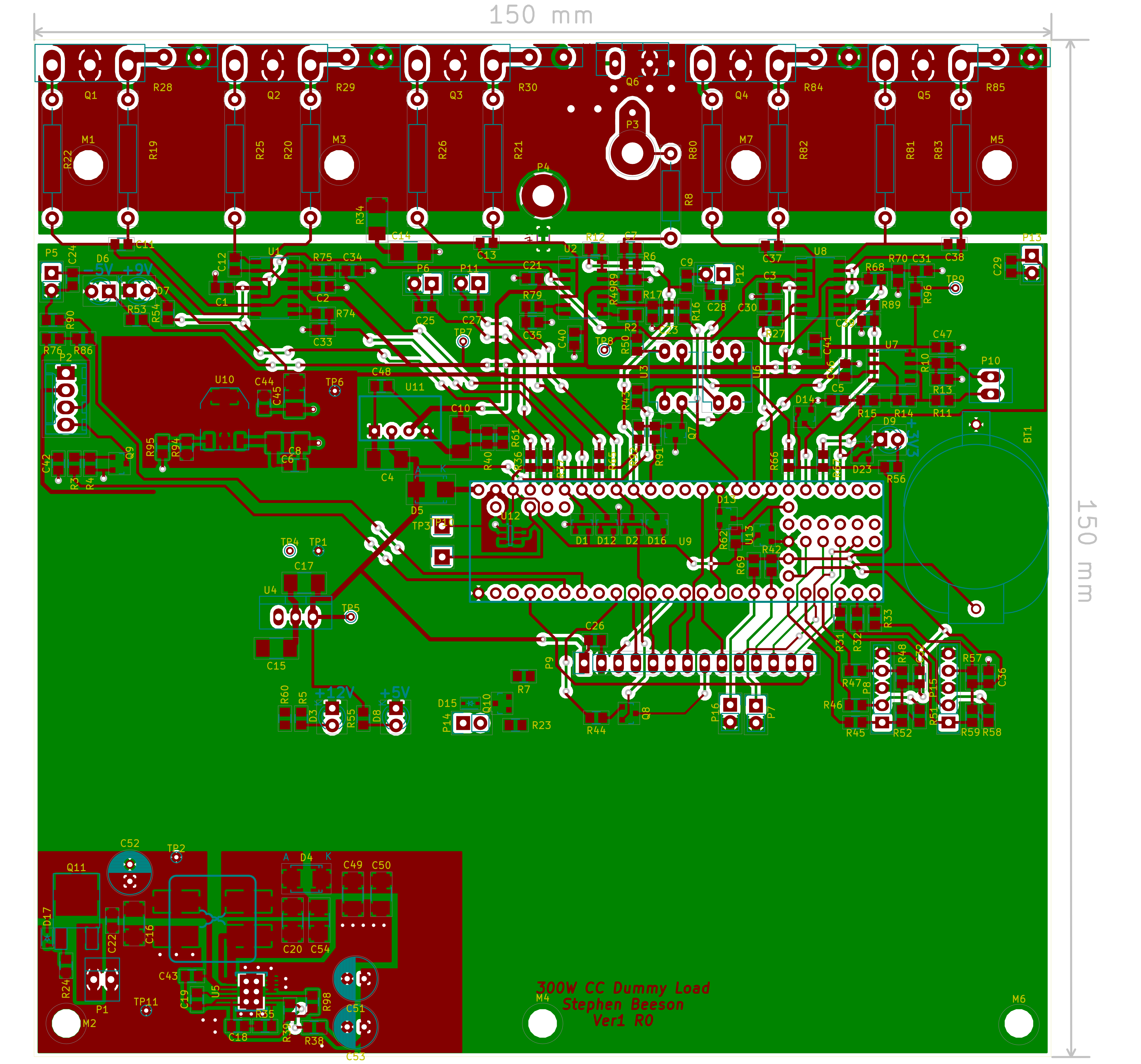
Picture of the PCB, max size is 15cm x 15cm, 15cm x 10cm was my plan but the new power supply took up more room and things are just getting to tight for my taste. Buying from Elecrow at 15cmx15cm size will cost about $11-$15 per PCB.
Removed resistor from FAN-PWM, found it was not needed. Also found that even pulling FAN-PWM low will not fully turn off the fans. May have to add an off circuit if I want to turn it off.
Going to try to space some of the stuff out, its pretty tightly packed together and I have room.
Picture of the PCB, max size is 15cm x 15cm, 15cm x 10cm was my plan but the new power supply took up more room and things are just getting to tight for my taste. Buying from Elecrow at 15cmx15cm size will cost about $11-$15 per PCB.
Brought the Pololu Sepic in to work and during break put it through its paces. From my tests it is vastly superior to the LT1961. I was able to take it all the way down to 3.25V input and 12.04V @ 481mA output with the tiny QFN TPS55340 reaching 72C. At 3.5V input it was 64C and at 4.5V it was 48C. In all I think I left it running on my bench for about 5 hours at various voltages.
The Pololu Boards TPS55340 is configured to switch at about half the frequency of the LT1961, but surprisingly the noise levels are very close to the same. The input voltage makes a huge difference along with the load. I think proper attention to the output caps will reduce noise even more.
Scope picture taken at 4V.
- Status
- Not open for further replies.