Decoupling caps, PCB layout?

Status
Not open for further replies.

Maggie

New member
I've been somewhat ignorant when it comes to the finer details of pcb layout. Recently I browse through a couple of books that try their best to make me clear. Here is a couple of examples of a recent board of mine, and I have highlighted three of the decoupling caps. The MCU is a LQFP100 package and the caps are 100nF in 0402 packages. The vias connect to ground and power plane.
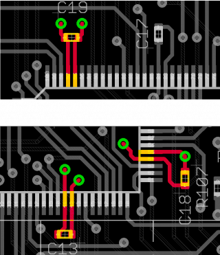
ua8wQ.png
The top cap (C19) is placed according to best practices (as I understand them). The other two are not. I haven't noticed any problems. But then again the board has never been outside the lab.
I guess my question is: How big a deal is this? As long as the tracks are short, does it matter?
The Vref pins (reference voltage for the ADC) also have a 100nF cap across them. Vref+ comes from an onboard TL431 shunt regulator. Vref- goes to ground. Do they require special treatment like shielding or local ground?
 
When you're not dealing with RF of HF, the placement is not that critical. Just keep traces short and grounding good. Judging from your two screenshots, the caps are placed just fine.

It is sometimes (most of the times?) a good idea to split analog and digital power and ground planes until the power supply. Digital and power electronics feed a lot of noise into the ground plane (or power drops in the power plane) causing small ripples in the ground (power) level which can affect the accuracy of your analog electronics further on. Most of the times I pour separate ground planes for digital and analog electronics and make sure that they are firmly connected to each other at the power supply ('star topology'). This way ripples in the ground plane coming from the digital part flow towards the power supply only in the digital plane.
 
I guess my question is: How big a deal is this? As long as the tracks are short, does it matter?
The answer is a little more complicated than one might suspect at first sight, but the details really only matter at frequencies of multiple hundred MHz and above. The position of the vias "behind" the cap, as implemented with C19, does not improve power supply impedance at high frequencies, but it reduces back-coupling of current pulses from the IC into the supply planes. So this is for EMI, not to enhance the supply quality as seen by the IC. This is often disputed, but I have never seen measurements or simulations that disprove this claim. I'm happy to change my mind if someone provides new evidence.

Regarding the trace length, I guess you know about the rule of thumb of about 1nH per mm of trace length. Two comments on that: First, do not forget the return path. Second: Try to visualize how the current continues to flow inside the IC. The package pins we see are ends of a lead frame, which connects to the silicon chip with bond wires. On most packages with high pin count the silicon is only a fraction of the packages size, so there is additional lead length inside the package, which is often several times longer than the PCB traces to the cap.

-Ben
 
I guess my question is: How big a deal is this? As long as the tracks are short, does it matter?

The Vref pins (reference voltage for the ADC) also have a 100nF cap across them. Vref+ comes from an onboard TL431 shunt regulator. Vref- goes to ground. Do they require special treatment like shielding or local ground?

It all comes down to the intended application. Hott and others will argue that running power lines through the cap before hitting the IC is best practices to keep noise from inside the IC from polluting the rest of your bus. However, even the Teensy seems to have a couple of power lines that connect to the IC on the "inside" of the chip and then run out to decoupling caps (i.e. similar to your lower drawing). They seem to work just fine.

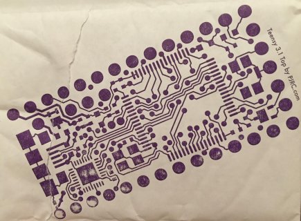
Osh Envelope.jpg

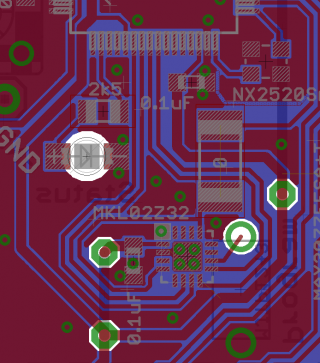
I go to great lengths to emulate best practices, including using external power lead jumpers or 0-Ohm resistors to avoid breaking ground planes (I only design 2-layer boards). Here is one example. Note: This design is BAD - two wires going to the MKL02 need to be swapped.

Board.png

Note the use of the 2010 resistor to jump "reset" over power and signal lines. Then there are multiple power wire jumpers visible as well.
 
Last edited:
> the caps are 100nF in 0402

Best to use the largest, reasonably priced value in the package size you choose (perhaps 1uF with 0402). The beneficial effect of this shows up clearly in tests.

You can get away with a lot - but best not to.
 
Careful.

Higher capacity ceramic caps have all sorts of issues re actual capacity vs rated as you approach the rated voltage.

Cap construction type, voltage, transient frequency, all play into which cap is best for a given application.

For example, IIRC, Freescale recommends a 0.01uF cap from AGND to each analog input to help minimize noise.

On the power supply side, I usually mix tantalum caps (10uf) for bulk storage with 0.1uf ceramic decoupling caps for power pins on all sensor, IC, etc. How much to use etc should be dictated by data sheet and/or experimentation with better gear than I likely have. C
 
Oh brother. Thanks for discovering that! I wonder why they're resorting to this... Should we report it as spam?
 
I've seen some first-time-posters recently that used existing threads to comment stuff like "hoping to learn more about this". Maybe they think the first comment is moderated? But this time they got me... So I guess we'll have to google-search sentences of first-time posters to detect stuff like this? Only takes a couple of seconds, so I guess we can deal with it. Let's see if the Maggie account will be used for spam.

Edit: Almost forgot: Thanks HWGuy!
 
Maybe linking this thread to the pool for future wiki entries will yield at least something useful from this spam?
 
Thank you

When you're not dealing with RF of HF, the placement is not that critical. Just keep traces short and grounding good. Judging from your two screenshots, the caps are placed just fine.

It is sometimes (most of the times?) a good idea to split analog and digital power and ground planes until the power supply. Digital and power electronics feed a lot of noise into the ground plane (or power drops in the power plane) causing small ripples in the ground (power) level which can affect the accuracy of your analog electronics further on. Most of the times I pour separate ground planes for digital and analog electronics and make sure that they are firmly connected to each other at the power supply ('star topology'). This way ripples in the ground plane coming from the digital part flow towards the power supply only in the digital plane.

Your reply is very useful!I think I can try it sometime.
 
Replies suggest human but it's clearly not a legit post. I guess the plan is to replace the harmless looking links to something else once the thread is idle. Either that or Kynix.com is getting desperate to improve its rankings.

Kynix said:
We adhere to honesty and ethics as our business philosophy...
... or not?
 
Should her name be change to ELIZA?

Dave: Open the pod bay doors, HAL.
HAL: I'm sorry, Dave. I'm afraid I can't do that.
Dave: What's the problem?
HAL: I think you know what the problem is just as well as I do.
Dave: What are you talking about, HAL?
HAL: This mission is too important for me to allow you to jeopardize it.
Dave: I don't know what you're talking about, HAL.
HAL: I know that you and Frank were planning to disconnect me. And I'm afraid that's something I cannot allow to happen.
 
Copying a question posted 5 years ago on another site? Maggie, it's not looking good for you. My finger is getting twitchy over the ban user button.
 
Status
Not open for further replies.
Back
Top