Teensy 3.5/3.6 Breakout board to test things with.

@mjs513

i guess the adapter shown in post #40
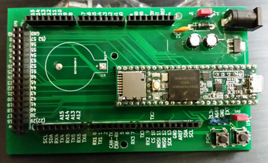
20170508_221235.png

is not published yet?

i could really use it for my 3d printer as it would allow me to interface the teensy directly to say a Ramps board or Ramps FD

without it i would have to modify the Ramps FD to accept the teensy, and that includes a risk of screwing things up big time
 
@boelle.. Sorry for the delay in getting back to you here. I just finished an updating the board and testing the new ones that came - haven't tested all the pins yet though. I still need to do a proper BOM. The one I used for the Kicad was really for the layout, schematic and footprints. Give me a day or two to do the BOM and I will post it to GITHUB.
 
:-D

that will be awesome as it will allow a quick compare between Due and Teensy

and i have heard rumors that a new Ramps 1.7 (or at least its post 1.6) should be in the works
 
what was fast????

your post does not quite make sense

That was a (fast) spambot ;) either reposting old posts or meaningless stuff to get a foot into the door for replacing that later with islamist hate speech, erectile dysfunction ads, porn, or other spam...
 
That would make perfect sense :-D

@mjs513: ahad any time to publish on github? and what is the address for the github repro?
 
@PaulStoffregen

btw.. i have been told that you once worked on a teensy based 3d printer controller or a shield

are there any truth to that?
 
Well, "worked" would be a strong word to use.

Years ago I did some early porting work on the Marlin code, but no hardware. More recently I may have asked someone to look into making a shield. So far, nothing to report there.
 
@PaulStoffregen

as far as porting the code you dont have to do that anymore

there are a pins file for the teensy 3.5/3.6 thou it does not have everything filled in


so its really down to the hardware side, that is one reason why i'm poking @mjs513 all the time for his adapter, it will allow me (i think) to insert the teensy 3.6 in his adapter and then add any arduino shield on top of it
 
Last edited:
@boelle

so its really down to the hardware side, that is one reason why i'm poking @mjs513 all the time for his adapter, it will allow me (i think) to insert the teensy 3.6 in his adapter and then add any arduino shield on top of it
Becareful with the power. It was really designed for the T3.5. However the power does go through the 5v pin that is connected to the USB power. The slide switch will allow you to go to USB power or the on-board regulator.


EDIT: Also make sure you check the pins out of the breakout board and any shield you use. I designed it so I could use some of the Arduino shields. I tried to keep the long edge pins the equivalent to the mega/due but do a double check. The 2x18 no guarantees since the board are different to the Teensy.
 
@mjs513

no worries, i planned to use it together with Ramps 1.7 (still in the works) that will work with the Due also, i just want to try the teensy as it s faster, has a FPU and mre memory

So power wise i think i will be good as power will come in from the shield and go through either Vin or 5V pin


But will print schematic and do a more close compare first before i start to look at the BOM
 
@mjs513

did a pin for pin check and there are a few connectors i'm not sure on

P8:

looks like it has been mirrored on the schematic - pin 1 should be the one towards P5 if not mistaken. if looking on https://www.pjrc.com/teensy/pinout.html that should be digital 57.

but its pin 2 on P8 that is connected to P10 pin 34 (52/57)

i thought for a second that i had confused myself but i cross checked by saying that the debug pins are furthest away from P5 and should not be connected, but on the board and schematic they are


P9: if using a teensy 3.5 its connected correct, but what could i do if i use a 3.6 ? simply remove the connections on pin 1+2?


P14: pin 3 is reset, its connected to P16 pin 4, that is not reset but 3.3V. Is that correct ?
 
@boelle

Looking at it now. I had to go look at the PCB board to check connectors. This was one of the first boards I did with KiCad so I didn't label the pins - my fault sorry.

Lets get orientation correct (doing this for me so I get it right). P11 is the right edge connector and P5 is the left edge connector looking top down. P8 is the connector for the underside pins.
P8: looks like it has been mirrored on the schematic - pin 1 should be the one towards P5 if not mistaken. if looking on https://www.pjrc.com/teensy/pinout.html that should be digital 57.
If you look at the flip side of the pinout card P11 connector is now on the left and p5 on the right. So pin 57 should be on the left side of the teensy towards p5. Think its right. Pins 1,3,5 7 are the debug pins and they are not connected.


but its pin 2 on P8 that is connected to P10 pin 34 (52/57)
Pin 2 on P8 corresponds to Pin 57 on the Teensy and yes it connected to the P10 connector (2x18) . Remember what I said I tried to keep as many pins the same as the Mega.


i thought for a second that i had confused myself but i cross checked by saying that the debug pins are furthest away from P5 and should not be connected, but on the board and schematic they are
They are not if you look at the schematic (they correspond to 1, 4,5,7 on P8


9: if using a teensy 3.5 its connected correct, but what could i do if i use a 3.6 ? simply remove the connections on pin 1+2?
Nope. pin 1 and 2 on P9 now correspond to A25 and A26 (corrected) for the T3.5 but for a T3.6 they are DP and DM (second USB) :) You just don't have the extra 5v pin.


Will check the last one in a bit have to go take care of something :)
 
Last edited:
@boelle. If you just need 1 board I have a bunch extras. Send me you address through the message on the this forum and I can send you one.
 
P14: pin 3 is reset, its connected to P16 pin 4, that is not reset but 3.3V. Is that correct ?
Nope. Reset is on P16. It is pin 1 on P16 which goes to SW3 and the other side of the SW3 goes to P16 pin 3 which is Ground.

Hope this answers your questions.
Mike
 
made a side by side compare

https://imgur.com/a/AARKfKn

on the right you have the pinout from https://www.pjrc.com/teensy/pinout.html

you can just barely see the usb plug on the right which also told me how to flip the image in my head to make the GND pad match up with the board in kicad

debug pins are towards the GND pad so they should be on the bottom row of P8

Pin 57 is towards Vin and 3.3V which means its towards P5 and P7

Pin 57 cant be towards P9 since that is the usb header and that one is shifted 1.27mm which is closer to the debug pins
 
Nope. Reset is on P16. It is pin 1 on P16 which goes to SW3 and the other side of the SW3 goes to P16 pin 3 which is Ground.

Hope this answers your questions.
Mike

i just assumed that RST on P14 was reset, and that it should be connected to reset and not 3.3V
 
Back
Top