Teensy 3.5/3.6 Breakout board to test things with.

KurtE

Senior Member+
As I mentioned in the K66 Beta thread #1128 and some of the other posts, I decided I wanted to make a quick and dirty breakout board that had some of the features I normally use, like 3 pin headers and the like.

Michael had a lot of good suggestions in the following posting:
Code:
KurtE: A couple of thoughts, feel free to ignore them:

    You might not want to put something behind the back of the Teensy 3.6/3.5 to allow the user to easily insert/remove micro sd cards;
    I found in putting headers on my 3.6 that the program key is hard to get to. It might be useful to break out the program pin just like you did with the reset pin;
    I don't know if it would be useful to change the 3x header rows to 4x. On the data pin side, it would be useful to bring out VIN (or possibly a separate power that defaults to VIN, but the user could specify their own). On the analog pin side, it would be useful to bring out Agnd and/or AREF.
    For a larger form factor, consider having logical breakouts in addition to the normal pin breakouts to bring out the 6 UART lines, 4 i2c buses, 2 i2s buses, 3 spi buses, 2 CAN buses). For the i2c buses, it would be helpful to have a way to solder in pull-up resistors.
    In addition to 5.5mm power jack, it may be useful to have a 2 pin JST header for connecting lipos. Having an area for lipo charger would be useful (perhaps setup for the Adafruit Pro Trinket Backpack).

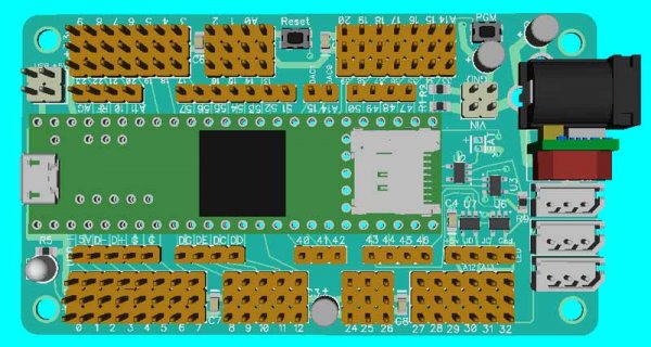
I hacked around some more on it to address some of the issues mentioned, plus add a few things, but so far tried to avoid adding the kitchen sink.

I added more room behind the back end of the board to hopefully allow insertions and removals of SD card.

I did not yet widen the board to allow me to choose additional power capabilities, like choose what voltage goes to the pins. Nor did I extend on the capbilities for ARef and AGnd. Note: those pins are brought out and labeled AG and RF.

I played around some with adding the JST connector and allow run from 1 lipo and maybe add charging circuit, but punted for now as I would not have +5v, not sure how best to power things, like probably separate powering of Teensy from other stuff. I did add a 2x2 connector with GND and VIN, so you can use those to jumper in or out of the board. My thinking is if you need this, the board should still be compatible with the stuff up on Tindie...

Added PGM button.

Added .127 2 pin connector area going to VBAT/GND to allow RTC battery backup. Not sure what part to use there, but this appears to be the size of connector of some of these batteries. Example ones from ODRoid.

One Kitchen Sink: I like LEDs, like Neopixels, So added on Two level converters (and gates like prop shield). Also used IO pins associated with SPI2 CLK/MOSI, so can use dotstar as well (I believe).

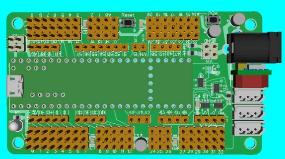
Board currently looks something like:
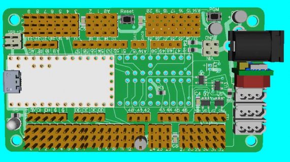
T363D-Start.jpg

There are more things I would like Sound... But not sure of best approach now, also would need to increase size of board to add speaker, so decided to wait on this to see what options we might have. So I ordered a set of 4 of these from Digistump, for about $24.

Now back to playing with the hardware and software.
 
For the fun of it I played around Autodesk Fusion 360 to see if I could update the Step file for Teensy 3.x I found earlier into something closer to the Teensy 3.6...

Here is updated picture.

T363D-Start.jpg

I might play around a little more iwth it and show some rectangles of major pieces, like CPU and SDCard.
 
Have you thought about castellated shields like FrankB's (https://pcbs.io/user/FrankB) or CPT's (https://www.oshpark.com/shared_projects/Gnvbt7io)?

Soldering on the header pins still gives me pause, as I don't (yet) have things like a reflow oven, and with just a soldering iron, it is easier to glob solder on the castellated shields. It may be I'm missing lots of basic

The Teensy 3.6 is more challenging to get things lined up, in that you have 3 groups of pins that need headers, and between two groups of pins are the 5 through hole pins.
 
Hi Michael,

I totally understand about soldering skills. It will be a little of a challenge for me to solder those 4 smaller ICs... I have two soldering units. An older WSL which I keep a finer tip on, and a Hakko which I keep a bigger tip on. I wish I had access to a soldering goddess :lol:

I thought or thinking about making a real simple breakout along the lines of FrankB's or the like, where you have cutouts along inside pads that you then solder directly to the Teensy.

My assumption with this type of board is I would be very limited on where I could run etch. That is I assume that there could not be any etch on the top, except maybe directly between the exterior pins, as to reduce the chance of shorts. Also obviously you can not run etch through the slots. Some of the things I wonder about making a board like this are?

1) Is the goal to make it such that I have access to all IO pins on a breadboard? If so the board may be something in the range of 4.5" long.
1a) Do you keep the order for the breadboard the same as the chip such that all of the other pins go to one end or potentially split between front and back? If so probably real hard to get all of those trace through...
1b) Or can you interleave. Either by pin or by group of pins. What I mean by group is for example on one side you might go:( GND, 0, 1, 2, 3, 4, 5, 6),( G, DE, DC, DD), 7, 8, ...

2) More like the board I have, where maybe things are broken out in 2 rows of pins on each side of the chip. Probably easy to create one like that, but again for breadboards you would only have access to half the pins...

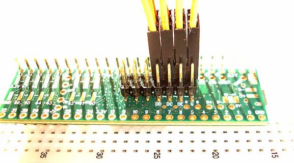
Now as for how I plan to try soldering the multiple groups of bottom pins is something along the line of:

a) setup a breadboard with extra long header pins like: https://www.adafruit.com/products/400
Where you have two rows of 24, aligned properly such that you can place the teensy 3.6 onto the board upside down and then use servo extension cables and shunts to help align things. Here is shown partially setup.

Bottom-pads.jpg

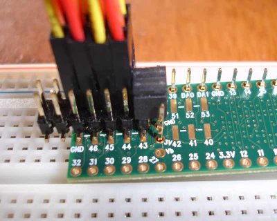
Update: 2nd picture showing the idea of using shunts as well
Bottom-pads-2.jpg

When I do this for real, Will have the right connector or a least cut to be right. Also for the other two with the 5 pin holes, I hope to have long pins stuck through some of them as well, and then use Shunts to connect to end pin of right angle connector and that row of pins, so then held in position in two directions. Not sure if that makes sense, but that is what I am going to try...
 
Last edited:
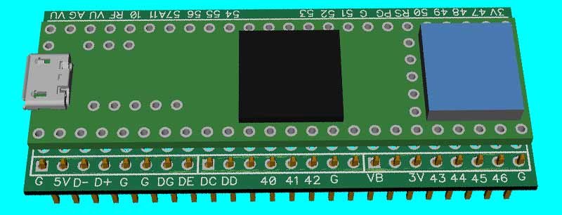
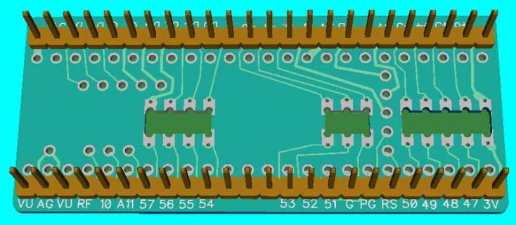
For the fun of it, I started a quick and dirty design, from the above, where all of the pins are arranged in double horizontal layout. That is you could use two 2x24 pin connectors...

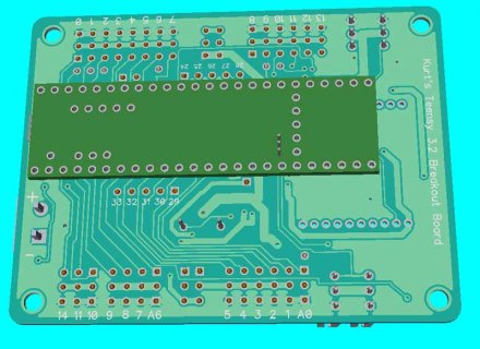
Not done yet. That is I have not actually routed it, nor updated the bottom to make cutouts. I was thinking on the cutouts, to extend the pads as rectangular pads, cut off from middle of hole, but add in another hole farther out, probably small vias, with the idea if soldered direct to board, the solder that flows under should make contact with the top pad and the via will help make sure connection made... Not sure if that makes sense.

T3.6Mini-Board.jpg

I could make it a little smaller but left room to add signal names...

Maybe something like this for cutouts?
T3.6Mini-Board-bottom.jpg
 
Last edited:
For the fun of it, I started a quick and dirty design, from the above, where all of the pins are arranged in double horizontal layout. That is you could use two 2x24 pin connectors...

That looks like a nice try for getting all the pins usably. I've had good results with the castellated access so far, though that Teensy board is now committed for life.

Actually soldering the pins can be a challenge - I took a breakoutboard version of T_3.1 and put female headers on top (to emulate the K66 Proto) and had blind solder in that case to the pins out the bottom with no way to solder the top where the header was - luckily I got solder paste in the holes in advance and it seems to have done the job. Would doing a second hole wide - allow soldering in that type case?
 
Yeah, I can imagine the castellated shield would make routing harder. And of course having more pins, makes it bigger which in turn makes the shield more expensive.

One thing that occurs to me, is it may be simpler to envision two shields stacking. On the bottom shield it gives access to the bottom pins brought out with 3x4 right angle headers (https://www.adafruit.com/products/816). The bottom shield would have holes for the traditional through hole pins, but no electrical connections (perhaps having a little bit of metal around the hole to be able to solder the pins to from the Teensy).

Then the top shield would be mounted on top of the Teensy and brings out the pins in various formations. Obviously you have to bring out the program button as a button because you would not be able hit it if you mount something on top.

The two shields would be completely independent. You could just use the top shield if you don't need access to the bottom pins, and you could just use the bottom shield and use a protoboard, or something like the sound shield mounted on top.

I tend to envision shields like this as experimental shields, where you are using it as an easier to use breadboard, where you have 3 or 4 wires come out for each PWM, sensor, etct. I tend to use Teensies in this fashion, where I build something, use it for awhile, get bored with it, and start over. In this case, the overall size is not as much of an issue (though the larger size making it more expensive is a factor).
 
Last edited:
Thanks guys,

I may play around some more with it, like probably expanding the slots. Like not sure if it makes sense to merge the two inner slots into one.

Also may setup some of the other unused pins, to maybe add more GND pins or 3.3vpins

May also shrink the board to not have room as much room on top for labels.

Then maybe order a few just to see how the look. Not sure if castellated boards would be easier to use if you make the board thinner? Example if .06, might be easier to get the solder to bridge around?

Defragster: Not sure if adding the extra vias will help or not, but I hope so. Before I order any I will try to print out a version of it at the same scale as a print out of T36 bottom to make sure things align properly.

Michael, lots of great ideas. Not sure if I will be the one to try to implement all of them as I am just doing it for my own fun. But hopefully maybe someone else can expand on it. I will also put all of my stuff up on github at some point so someone might be able to use it as a starting point.

Then at some point soon will play around some more with the idea of how would I modify some of my current boards to make use of the 3.5 or 3.6. Not sure yet if it would imply one or multiple boards.

Example for the Trossen hexapods that use AX or MX servos, All of the servos are controlled through one serial port, with probably the added stuff for conversion of 3.3v to 5v. Probably one that uses direction IO pin, but can do with half duplex support.

But may want one to try out on my old Lynxmotion RC servo based robots, which require that has lots (18 or 24 +) of 3 pin Servo headers (extension of the test one I have ordered now), where I can direct Servo power to these pins. May want to look if it makes a difference on which IO pins to use. If I get real ambitious (not likely) could do like some servo controllers and use multiplexers which are driven off of Timer IO pins for very accurate RC output.

But as you sort of alluded to, there are lots of other capabilities that would be fun to play with and still is the question of do it you build it into the main board, or do you build hat(s) for the Teensy.

Example: XBee: Takes up lots of room, could simply use the XBee adapter: https://www.pjrc.com/store/xbee_adaptor.html

Sound: Audio adapter - How much of it is needed on T3.5/3.6 which has SDCard on it. How hard would it be to make a breakout with just the needed parts?

Now back to playing
 
Just a passing note - one useful thing would just be DEBUGGER half unit. If you made it in two part one debug and then the rest, they could be ordered cheaper and used selectively?
 
BTW, for people looking at generic protoboards, I just got a new mint tin shaped board from Azzy's Electronics in tindie (https://www.tindie.com/products/DrAzzy/mint-tin-size-prototyping-board/) that looks pretty good. I bought 4 boards for $16.75 including US mail shipping.

Unlike the Adafruit mint tin perma proto (https://www.adafruit.com/products/723) which is laid out in standard breadboard fashion, the Azzy board has various 2, 3, and 4 row headers, ground pins on all 4 sides and in the middle, and a power strip down the middle. From a Teensy perspective, it would have been nice if he had brought out 2 more power rows in the middle for AGND and VIN, sacrificing one row on each side. Or maybe even a 5th power rail for external power.

But for the 3.6 through hole pins, I can imagine breaking out the 3 i2c buses, each on a 4 pin row, to allow plugging 3 separate i2c devices in each bus. For the 5 serial ports, I would put them in the 2 row headers (one to connect the wires, one row for the serial port header). The 2 SPI buses would probably go into the 3 row headers.
 
Last edited:
Sound: Audio adapter - How much of it is needed on T3.5/3.6 which has SDCard on it. How hard would it be to make a breakout with just the needed parts?

Now back to playing
Lets see, for the sound board if you use the software as is (i.e. being restricted to using Teensy 3.2 pins), you would need:
  • Pin 6 would not be needed unless you also want to access the on flash memory that can be soldered to the board;
  • Pins 7, 10, 12, and 14 would be needed for SPI (7 is alternate MOSI, 14 is alternate SCK) -- now, I think the only SPI things the sound board does are flash memory and micro SD, so you might not need these pins;
  • Pins 9, 10, 11, 13, 22, and 23 are used for i2s (possibly use 2nd i2s bus if you are willing to change the software);
  • Pins 18 and 19 are the first i2c bus (audio board has 2 i2c devices);
  • Pin 15 is the analog device you can solder on the board for controlling volume.
  • I assume you need to connect ground, 3.3v, vin, and agnd.
 
Just a passing note - one useful thing would just be DEBUGGER half unit. If you made it in two part one debug and then the rest, they could be ordered cheaper and used selectively?

I've asked a couple of times but still not know which debugger would be good..
 
Thanks again,

As you mentioned, might be able to break it into two pieces the front and the back.

I decided after playing around a bit, to order a see how well they might fit. Already I redid it a bit as I used the picture of back of Teensy, plus output an image of the layout, and then brought it into Photoshop (still on CS2...) sort-of stretched and moved to line things up and saw, I should move the pads and the like.

From digistump, was about $10.50 for set of 4 including tax. I figure I have awhile to try it out as the kickstarter units are still over a month away..

I think it is a little closer now.
T3.6-breakout-overlays.jpg

If I like the idea of using them, may look into other things like cutout around host/device select.

Kurt
 
Thanks Michael,
Lets see, for the sound board if you use the software as is (i.e. being restricted to using Teensy 3.2 pins), you would need:
  • Pin 6 would not be needed unless you also want to access the on flash memory that can be soldered to the board;
  • Pins 7, 10, 12, and 14 would be needed for SPI (7 is alternate MOSI, 14 is alternate SCK) -- now, I think the only SPI things the sound board does are flash memory and micro SD, so you might not need these pins;
  • Pins 9, 10, 11, 13, 22, and 23 are used for i2s (possibly use 2nd i2s bus if you are willing to change the software);
  • Pins 18 and 19 are the first i2c bus (audio board has 2 i2c devices);
  • Pin 15 is the analog device you can solder on the board for controlling volume.
  • I assume you need to connect ground, 3.3v, vin, and agnd.
What was sort of wondering is if you remove all of the extra stuff, would it make sense to maybe make a "Sparkfun or Adafruit like" breakout board, for the needed components.

But maybe not if it would likely have issues with noise or the like? Also as mentioned if it takes somewhere like(4+6+2+3+) or about 16 pins, maybe a pain to route all of these remotely on a board.

My question to myself (as well as others), is suppose I am designing a board to use, mainly for my Robotics, but also maybe some more general purpose as well. What approach to take to add functionality like sound, Neopixels/dotstars, TFT display, maybe IMU, maybe XBee or maybe RF radio... Sometimes may want to use the board standalone and other times slave to Linux box. Obviously one approach for several of these is to use either Audio board or prop shield. But was wondering if it made sense to make a T3.5/3.6 specific version of some of these.

Or should I add some of the components on my own board. If so may play around more with Prop shield sound as on many of these boards before I simply had simple RC circuit with buzzer, which I could make simple beeps or the like. Probably need to think more about this.

Side note: Thought about trying to order some reasonably quick version of the small breakout boards that are .6mm. So thought I would look back up at the place I first did PC boards, which is PCBFabexpress, so if you try to order these small boards which are something like 2.5"x1.1" and get three of them in 3 days, you can order them for about: $159, you can get them cheaper with 10 day ordering for only: $108 8) And these only come with silkscreen on top. If you want it on both sides, then you add $50... I think I will stick with Oshpark, Digistump and Seeedstudio.

Kurt
 
I'll make a board with ILI-Touch Display, MPU9260, Lipo-Charger and sound with PT8211 (I2S, Stereo). I'm a bit undecided if i add a stereo-ampilifier or not
I've never soldered such a small part like the MPU9260, so i'll try the oven-approach this time..
 
I'll make a board with ILI-Touch Display, MPU9260, Lipo-Charger and sound with PT8211 (I2S, Stereo). I'm a bit undecided if i add a stereo-ampilifier or not
I've never soldered such a small part like the MPU9260, so i'll try the oven-approach this time..
Sounds like a fun board. I have avoided small tight pin chips up till now. The 4 to the right of T3.6 are enough of a challenge for me:
T363D-Start.jpg

Right now I am thinking that for sound maybe a mono amp like on the Propshield would be sufficient. And maybe mount something like a CBS-1508 small speaker on the board. I have been thinking of trying a toaster oven approach with maybe one of my boards try ordering a stencil and... Anyone have suggestions on easy setup for this. Like which solder paste to use, that is good for novices?

Thanks again
Kurt
 
I've asked a couple of times but still not know which debugger would be good..
In fact,
after so many requests to have the possibility to debug, I'm surprised that no one is discussing HW and SW solutions for T3.6, which makes me think the debug feature was only requested because it did not exist on T3.2
 
In fact,
after so many requests to have the possibility to debug, I'm surprised that no one is discussing HW and SW solutions for T3.6, which makes me think the debug feature was only requested because it did not exist on T3.2
I think the main reason it has not been talked about more yet, is a lot of people may not know what to ask. As you mentioned what hardware units work. Then can you somehow use it with Arduino stuff or do you have to go to some other setup... But hopefully after the kickstarter is under control, Paul will come up with a complete answer.
 
Paul mentioned a proper way for debugging, integrated into the Arduino IDE, is on his to-do list. Maybe this will use JTAG as well?
 
Right now I am thinking that for sound maybe a mono amp like on the Propshield would be sufficient. And maybe mount something like a CBS-1508 small speaker on the board. I have been thinking of trying a toaster oven approach with maybe one of my boards try ordering a stencil and... Anyone have suggestions on easy setup for this. Like which solder paste to use, that is good for novices?

I've had good luck with just an old electric griddle (i.e. a pancake griddle) we have knocking around here (note: don't use it for food ever again!). Stencils from OSHStencil. I bought a tube of Chip Quik solder paste (they have a ton of options, finally I just bought this to try and it's been fine - there are lead-free options if you want). Preheat griddle to ~350F, put thin piece of aluminum plate onto the hottest section (the one I use only barely gets to 425F in the hottest section which is barely hot enough in my experience to do the job, and has a lot of cold spots - the aluminum plate evens some of that out so the board gets a semi-uniform temp). Apply solder paste with stencil: jig up board with stencil, squeeze some paste onto the board/stencil near the pads, swipe once with the card that comes with each OSHStencil order, hopefully getting good coverage on all the pads. It takes a few tries to get used to it, if you mess up, isopropyl alcohol cleans the board right up for a new try. Then I place chips (usually the hardest part, my hands aren't the steadiest but I've managed), and carefully put the board onto the aluminum plate on the griddle. Turn heat all the way up (which is ~425 on mine), watch until things reflow. The largest chips usually "kick" last. Remove board (usually onto a block of wood), let cool. This may not be the best method, but it is quick and simple and has worked fine so far. Some day I might mod an old toaster so I can do a proper temperature curve.
 
Paul mentioned a proper way for debugging, integrated into the Arduino IDE, is on his to-do list. Maybe this will use JTAG as well?

- Maybe we cam use an other IDE as intermediate step. The question is, which hardware to use.. i have an st-link v2 somewhere. would it work ?

- Can we program an other teensy as SWD/JTAG debugger ?
 
Last edited:
k66 Teensy 3.6 Debugger

Just a passing note - one useful thing would just be DEBUGGER half unit. If you made it in two part one debug and then the rest, they could be ordered cheaper and used selectively?
I've been searching in vain on KS and the forum here for K66 Teensy 3.6 debugger and JTAG information. Is there a JTAG connector? Also I hope a real hardware reset input is there too. Debugger: don't think I care if integrate with Arduino. At the moment we only use Arduino to build and load, not to edit. Then we have to dispatch HEX files to customers and they will use TyQt to load. We use the ELF to get back some symbolic table information. Getting the HEX and ELF files is a hassle so I'm wanting to get a cmake build working. So a JTAG debugger with its own interface is fine. Segger says they have sold over 400,000 JLinks so presumably they have a good SW solution too. We are happy to help out with this if there is a way to do so. Just ordered a multi pack on KS, wish the Ethernet adapter was not sold out or we could order some at OSH Park. My TODO list is getting out of control...
 
Last edited:
- Maybe we cam use an other IDE as intermediate step. The question is, which hardware to use.. i have an st-link v2 somewhere. would it work ?
- Can we program an other teensy as SWD/JTAG debugger ?

JTAG is much like SPI and the HW is very simple, or at least can be. There are a ton of cheap JTAG adapters out there already, in fact we made one back in the day and sold a few hundred for use with Xilinx parts and an embedded Java controller we sold, so the HW I pretty much grasp. The SW is the issue and I am pretty ignorant about the standards there. Some of the low cost debuggers are specific to a given manufacturer, but AFAIK the generic JTAG will work with pretty much any device as long as the PC end knows how to talk to someone's SW, thought the inevitable "standard" USB connection to a PC.

If I had a way to connect to the JTAG on Teensy 3.2 (pins are shared by loader as I recall so not so easy) or the new 3.6 (got in on KS but that will take a while) I would try some and report back. We have several Atmel JTAG (some old), an AVR Dragon, and newer JTAG pods in hope of being able to use a HW debugger with Teensy sometime soon.

To Paul's credit we have gotten by without one pretty well. Sometimes we need a scope or I2C or SPI analyzer to figure out where things are not going as planned.
 
As I mentioned in another thread, on the Kickstarter I choose one that included a couple of t3.5's as I think this might be a great chip to try to upgrade older boards that may still require 5v tolerance.

On the Trossen forum a member asked about adapting one of our existing boards for the T3.2 to use a T3.5 or T3.6. There is an issue with size, as the extra inch but had the idea of maybe mounting it below the board, like:

T3.6-in-XBee-board-below.jpg

Which might work. However on this board I used the surface mount pins on the T3.2. So made me think about maybe should make an adapter board, that maps the T3.2 pin locations to T3.5/T3.6 pin locations. Maybe something like:
T3.6-T3.2Adapter.jpg

It may not be prefect, may work pretty well for boards like this.
 
Prop Shield to Arduino Shield

Hi KurtE

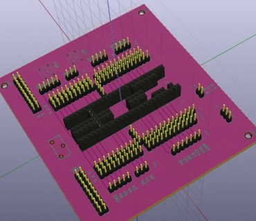
Hope you don't mind me jumping in on this discussion but I wanted to say nice work. Think I like two suggestions by MM on grouping the Serial, i2c, spi and can connections. I tried my hand at designing a basic breakout board (first time using KiCad or anything like it for that matter) its a big board but I wanted a basic board to experiment with. I added a battery and broke out the reset pins like you but I also added those fancy connectors to get access to the pins on the underside of the board like the one on Tindie (have a couple of those). I ordered the minimum from OSH park but have not received them yet (4 layer - told you didn't know what I was doing). I am attaching a image from kicad. I have no idea on powering from onboard supply so all the power would come from off the board. Not sure if I needed any diodes or the like so you all have any suggestions let me know please.

Mike
Capture.JPG
 
Last edited:
Back
Top