Playing around with RPIish HAT using Teensy 3.5 or 3.6...

Status
Not open for further replies.

KurtE

Senior Member+
As I mentioned in the K66 beta thread...

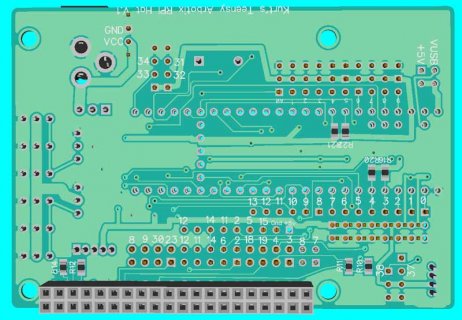
For the fun of it, just starting to play around with my Hat board (that could plug into RPI or Odroid or UP board), to use either the T3.5 or T3.6. Right now just playing around with ideas.

So far I dropped the BNO055 IMU plugging directly into board... I also changed Sound from using simple transistor RC circuit to try out using a simple AMP setup like LM483, with real simple speaker. Still have Neopixel, but may change?

Still want to hook up more configuration/communication options between Main board and Teensy. Like using more shunts to hook up UART between the two (actually still there). But also add ability to connect SPI between the two and maybe I2C...

Right now just getting ideas of space.

https://forum.pjrc.com/asset.php?fid=7500&uid=36542&d=1473357007 T3.6-RPI-Hat.jpg
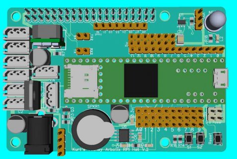
For example do I try to add space to back to Teensy for SDCard insertion. Or maybe mount Teensy high enough to go over top of connectors when no wires are connected...

Decided to create a new thread, will continue with comments made in other thread.
 
MichaelMeissner said:
KurtE, in terms of communications, it might be useful to have for the 3 main serial ports, the main CTS pin (and perhaps another pin for RTS). I picked up an Adafruit BLE board, and it wants CTS/RTS connected.

For i2c, consider having an option to connect pull-up resistors. It also would be useful to have several parallel rows, so that you could easily attach several i2c devices to the same chain.

For spi, consider also having several parallel rows, with the various CS<x> pins, so you could more easily plug in two different SPI devices on the same SPI bus.

Have two or three places you can add a push button. I used to use pin #2 for the generic push button, but now I use pin #3, since it isn't used by the prop-shield, audio shield, and the feather/OLED shield has a button for pin 3.

I think you now have a 2.1mm power jack. It may be useful to have a JST/charger option. The Adafruit Pro Trinket Lilion/Lipoly backpack is perhaps the easiest to use for through hole soldering (https://www.adafruit.com/products/2124). One thing that it would be very useful to have is the ability to switch power sources and cut off the power (this requires the user to cut the pad between Vusb and VIN).

Hi Michael, thanks for the feedback.

Yes, I do want to put in some more of the IO options like you mentioned. Right now trying to figure out what I can fit in this space, which is pretty much the size of an RPI, where the header shown on the top plugs directly into RPI (or in my case more likely Odroid and UP) boards.


Power: Yes I have one main power plug. With these boards I will normally be powering it with 3S lipo (11.1v) and if someday I have a setup with MX servos than may use 4S lipo. I show 8 Bioloid connectors 6 for the 6 legs of a Hexapod, another for the logical Head. These 7 connectors are controlled by big Transistor which allows me to shut off all power to the these servos. The 8th connector is directly connected to main power, so can have one or more things on the Bioloid buss even if I turn off power to other servos. I am also hoping to power the main board through this connector, I have it setup to use a 6 or 10 amp DC to DC converter, which should hopefully allow me to feed lots of power to the host through the connector. I do however want a secondary connector, actually the 4 pin connector to the right of 2.1 is actually only 2 pins, forgot to update the 3d model for the part. but am thinking screw terminal might be better.

Buttons and LEDS: Right now I have three buttons on it. One connected to Reset, and two others connected. Makes me wonder. Currently have these setup as Resistor ladder to one Analog pin, but with all of these pins, maybe convert to just normal digital pins. I also have another pin connected up for USER led and also setup for Neopixel, with option to put one on board and chain off of it.

My Question to myself, is how much of each boards pins do I wish to better expose on the board. For example the UP boards 40 pin connector has:
1 UART: TX, RX, CTS, RTS
SPI - with Two CS
I2C...

And how much of the Teensy to expose. Example: I can hopefully set it up for one of my Quick solder double rows.
T3.6-T3.2Adapter.jpg
By then adding room for double rows, then regardless that I don't use any of those pins, have the option to gain access to all of these inside pins. But that eats up a minimum of anther .2" space on the board... Not sure yet.

But hopefully I will have room for this, plus adding more room to break out some of the interfaces like you mentioned.

Also I am thinking about redoing my usage of IO pins. That is I use a lot of the lower pin numbers to talk to the different devices. Like I am setup to use RX1/TX1 from pins 0, 1 to talk to Host, likewise RX2/TX2 I use Pins 9, 10 to talk to the AX Servos and pin 2 for direction chip and 3 for turning AX Power on and off. I am probably going to move many of these up to higher pins.

Lots of stuff to play with. Will upload new version when I incorporate more of this. Also right now I have my own DIPTRACE parts defined for T3.5/T3.6 which is pretty messy. I have about three versions (one with the basic pins, like I show, another with the bottom pads added, and another one with it setup for cutouts... Trying to decide if to stick with my own versions or with Diiptrace I can use Eagle to convert the ones made for Eagle into script, which I can then import into Diptrace...

Thanks again!
 
If you are going to put neopixel/ws2812b or dotstar/apa102 support in, it would be useful to have VIN out as well as 3.3v, to allow for doing voltage translation (or add a place to solder in a 74AHCT125, and select several pins to bring out -- with 17/A3, 13, 11 being possible candidates, since those were used for the LC (17) and prop shields (13, 11).

However, I'm beginning to wonder if an all-in-one shield while useful in many cases, will cross the threshold in terms of larger board and make it too expensive. It may be useful to think instead of having a basic shield with a dense breakout of the pins, and then one or more daughter cards that would be connected to that dense breakout, and bring out selected pins in easier to use segments. Maybe something that puts out a 2x29 set of pins (with all of the important pins in the first 2x20 area, so you can use the common raspberry pi 2x20 cables to attach the daughter boards, or two sets of connections with a separation to allow for cables, etc.
 
Thanks again,

Yes the the Neopixel, I currently have one SN74LV1T125 on the board (U1) near the Neopixel, which is doing voltage translation to 5v and I am passing +5v, GND, and DOUT of the Neopixel on the board on the 3 pin connector. Again as you are mentioning, wondering if I should instead or in addition bring out some more pins. So I could potentially use dotstar instead. The only thing with Dotstar is so far I have not seen any individual one that you can use like the sell for Neopixel....

As you mentioned, if you add too much stuff the board can get too big and costly. Luckily I want to stay near the size of an RPI. I am already semi cheating as far as HATs are concerned as I extend over the USB and like ports. With the UP board this is probably preferable to leave an air gap for heat. But may consider putting some stuff on bottom if it makes sense and does not get in way. Example maybe small battery holder for RTC clock. But maybe not if Host already keeps time.


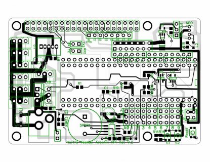
I have thought about maybe rotating the Teensy 90 degrees, but the Teensy is longer than the board is wide. Also trying to decide if I should leave the RPI connector area clear as to allow stacking? I may cheat a little more and maybe add maybe a .25" to the width, to make things fit easier. Especially if I go with the double row board idea. As you can see in the layout, that really crowds things up:

DipTrace-PCB---Teensy-Arbot.jpg

Again I have not updated much yet as still just playing on how much can you cram into a small space. Will probably punt on some options. Or maybe see about using smaller pinouts for jumpers between RPI/Teensy...
But probably back to drawing board.
 
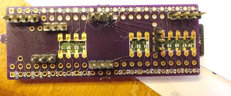
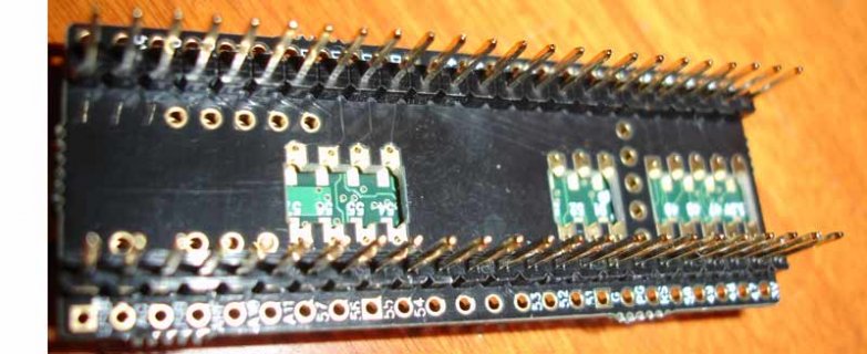
FYI - I got back my first cut at trying to make a solder on adapter to convert all of the bottom pads and the like to just two rows of pins.

I marked in some cutouts, but my guess is that I did not make them big enough to work easily.

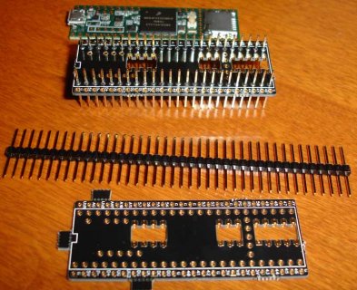
Here is a picture showing one with a T3.6 under it.

Adapter.jpg

With the picture, I just used several 3 pin servo extension pins, to help align things and also as a quick test to see if I properly laid out the locations of all of the holes.

Also not sure yet if it was the best idea to also move all of the drilled pads also out to the 2nd row as that implies I need to solder the pins to both boards...

Again it give me more options to think about.
 
Thanks Frank,

Yep it looks like one of them I accidentally moved a little off center. The other two were. Also it looks like I should extend the cut a little as the cut sort of rounded around a bit. I might try updating them and try again, as they are pretty cheap.
 
I have been playing around some more with the design. Right now I don't have it routed at all, but just getting an idea of just how much I can cram in...

DipTrace-PCB---Teensy-Arbot.jpg
I went back and forth on using the double pin setup, as it may help later if we have debugger support...

But I think I have enough stuff on this to play some. Assuming I can route everything. The resistors on the back or optional PU resistors for I2C. I have 8 of them, as I have two I2C interfaces shown for both Host and Teensy.

Communications between Host and Teensy
1) USB - can still plug it in to one of the USB ports
2) Serial - Have TX/RX/CTS/RTS - setup between the two (optional jumpers or can use each for other things)
3) SPI - Have MISO/MOSI/SCK and 2 CS pins. The Miso/Mosi pins are reversed for Host/Teensy so can jumper
4) I2C - Have Two I2C interfaces from each. Mentioned PU resistors earlier
5) GP - Two other GP pins between the two. Note: many of the ones in other sections can be used as GP pins as well.

Feedback for User:
1) Speaker - Setup to use LM4862M connected to DAC0 - hopefully will work OK...
2) Buttons - 2 buttons now on own IO pins
3) Leds - 2 normal Leds on own IO pins
4) Neopixel/Dotstar - I have two IO pins SN74LV1T125 chips to bring up to 5v. One of them goes to connector that can plug in Neo-pixel where the output can go to other connector (4 pin), the 2nd IO pin goes to 3 pin connector. The IO pins chosen were 37/38, which are also SDA1/SCL1, so can hopefully also use for Dotstar

I have 4 pin connectors for Serial4 and Serial5...
Also since I printed out this layout, I tried to squeeze in a 9 pin connector just below SPI, with the connections for ILI9341 display including resistor for background. Still playing, but
sure is tight.
 
Last edited:
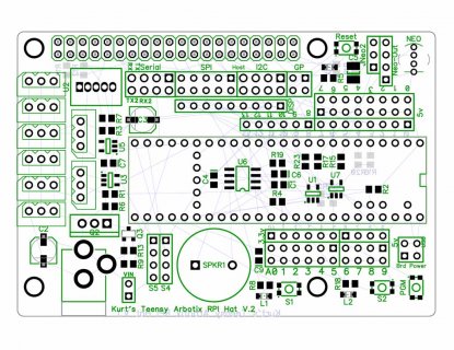
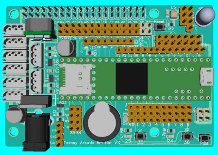
I played around some more yesterday and was able to route everything. I did rearrange slightly and decided it was probably good enough for me to try out, so ordered a set from digistump. Hopefully they will be a bit quicker than last order...

T3.6-RPI-Hat.jpgT3.6-RPI-Hat-Back.jpg

Note: There are a few 3d models that are not correct for pins, as for example did not have one for 1x9...

There are several things that would be nice to add, but I punted this round, like direct connections for Lora or XBee or the like, plus maybe backup battery. But for this round probably good enough to do experimenting with...

Edit: In case anyone is interested, I have the double row of jumpers between the RPI connector and the Teensy setup to use shunts to be able to setup different types of communications between the Host and the Teensy. Like Left to Right: RPI Label (pin number) : Teensy Label (pin...)
Code:
[B]Serial[/B]
RX(10) : TX2(10)
TX(8)   : RX2(9)
CS - CTS(36) : D30 
RS - RTS(11) : D23

[B]SPI[/B]
MOSI(19)  :  MISO0(12)
MISO(21)  : MOSI0(11)
SCLK(23)  : SCL (14)
CS0(24) : CS0-1 (6)
CS1(26) : CS0-0 (2)

[B]I2C[/B]
SDA0(3) : SDA0 (18)
SCL0(5) : SCL0 (19)
SDA1(27) : SDA2 (4)
SCL1(28) : SCL2 (3)

[B]Couple Extra GP Pins[/B]
(35) - D8 - TX3
(37) - D9 - RX3
 
Last edited:
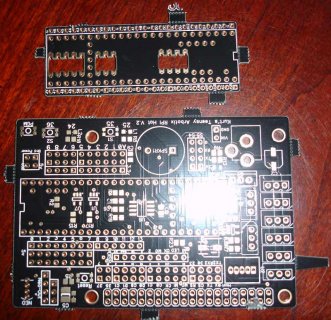
Thought I would mention that yesterday I received some boards that I had fabricated at Digistump. Actually two orders. One being the board above, the other a slightly updated board to maybe solder directly to bottom of T3.5/6 that breaks out all of the under pins to double row of IO pins.

T3.6-RPI-Hat-brd.jpg

Now I need to order some parts to populate one of these to see what works and doesn't...

But in the picture I wonder which board was above mine here when they were cut apart as I have parts of some pads here...
 
YEAH - and look at your big board lower corner - you got torn up too!

I've gotten a few boards from PCBS.io and never seen such breakage! You should send Erik that picture.

Let me know if the castellated board works - and if you can share the board, I'd like to order.
 
Kurt, are you sharing the board with the cutouts at pcbs.io or are the eagle-files available ? I'd like to order it.
 
The stuff is on my main machine, which I should be able to get to later today, and will make it available. I will upload design to github (Diptrace), plus gerber files and will mark it on digistump as shareable. My be awhile before I can try it out.

Defragster: yes I need to take a better look through the boards and find out how many of them may have been impacted.
 
But in the picture I wonder which board was above mine here when they were cut apart as I have parts of some pads here...

It looks more like the top board was coupled to the bottom board in your image if you ask me. The lifted pads on the bottom look to match the extra on the top board, and the second set of mouse bites (to the left) look like they match on both boards too. Either way, ouch!
 
Assuming that means you tried one and it works :) . . . . opps not tested . . .

PCBS.io Order placed! Under 9 bucks with tax for 4 boards. Hopefully in good shape - as is usual!
 
Last edited:
Yesterday, after playing with the UP board, I decided to try building one of the castellated mini boards I showed up above.

Short answer: For me, I think the board has issues, that I am not sure the best way to proceed and in the end may be more trouble than it is worth.

Now longer explanation:

Parts:
T3.6-castellated-parts.jpgT3.6-castellated-parts.jpg

I am using the Adafruit long pins, such that they can easily go through both boards on one side and on the other still have full length pins to use.

A major issue, is for several of the pins I need to make solder connections on both the T3.5/6 and the adapter board. Example inner pins, plus some of the GND and +3v.. So how do you do that?

If you assume that adapter will be flush with the spacers on the breakout pins, like shown:
T3.6-castellated-bottom.jpg

It is pretty hard to solder on this side of the board. So I soldered in on the other side, but knew this would probably be an issue. As once you do that it is pretty hard to get the solder totally flat to top of pads and once you do this and then try to setup to connect the two boards like:
T3.6-castellated-gap.jpg
You will most likely end up with a gap between the castellated pads of adapter and the surface mount pads on T3.5 (in this case). The gap could be easily larger than you can easily get solder connection between.

And assuming I got that to work, would then need to make the inner pin connections. Could have setup like I did the ones shown, which would add to the issue. Or if I was able to get the main parts to work, could solder wires through on both sides. Or could use pins like I was showing, solder on top, try to pull off spacers and solder and optionally put spacers back on... Could maybe do that for pins I show soldered above...

But I then ask myself is this easier and less error prone than simply using surface mount connector? Maybe not...

Options:
a) punt - which I will currently do and start to assemble the RPI hat board.

b) Assemble one, but don't make any pin solder connections between boards. This would cause some of the outer pins not work, like the A10..., DAC, PGM, RST, some Gnd and power pins... But at least all of the Surface mount pins would work... May try later, or if some one near me wanted to try...

c) Make a new board or boards that do not make these pin connections. Like maybe one for the USB end, which does that first set, Maybe offset down a bit to not be in the same space as the USB host pins. Then maybe one for the other end that does the other end.. Or could be three of them, one for each set...

d) make a Breadboard friendly version, which brings all of the pins out to one end or both ends, and have them align with the main pins, but not sure I would want a version that is maybe 4" long...

But for now :( punt!
 
You know that those black plastic spacers are removable ? With a bit fiddling it is possible to move them higher or to completely remove from the pins. Edit: after soldering.

2016-10-08 16.56.37k.jpg

BTW: normal length headers
 
Last edited:
You know that those black plastic spacers are removable ? With a bit fiddling it is possible to move them higher or to completely remove from the pins. Edit: after soldering.
Thanks - I sort of mentioned that as a possibility above... Sometimes I like the long pins as it allows me to easily hook up Logic Analyzer to pins...

Good idea to solder first to Teensy on top, remove spacers, and solder on bottom of adapter... Will be fun to see how hard it is to get the 24 pin spacer to move... Could of course use multiple smaller ones...

If I were using this to then connect to real board, I think I still want spacers between this group and the board, to make sure I don't have issues with etch/vias below, but probably just having the spacers on the outer row would be sufficient. Thanks

But again for me, wondering if this is simpler than using surface mount connectors, especially since it will eat up more room on the board.
 
Yes this is troubling - I noted my experience putting a very similar T_3.1 on a breakout board with female headers on top back when first PROTO K66 shipped.

With female headers - you can't move the plastic and solder later so much. When I put them together I put solder paste into each pin hole. Soldering the bottom that gave flux and solder with heat and solder from above it seemed to work. It didn't have to 28 times - 48 times would be more of a stretch - and too much paste could have been bad too.

for d) - yes 4" long or Franks Connector board style not breadboard friendly only 3" with 6 added stacked rows of 7, and I noted this elsewhere - castellate the side pins so they can be soldered from the edge
 
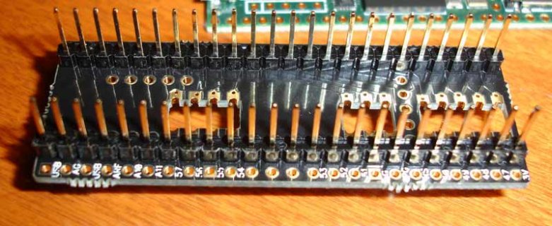
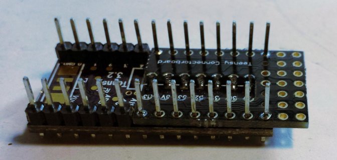
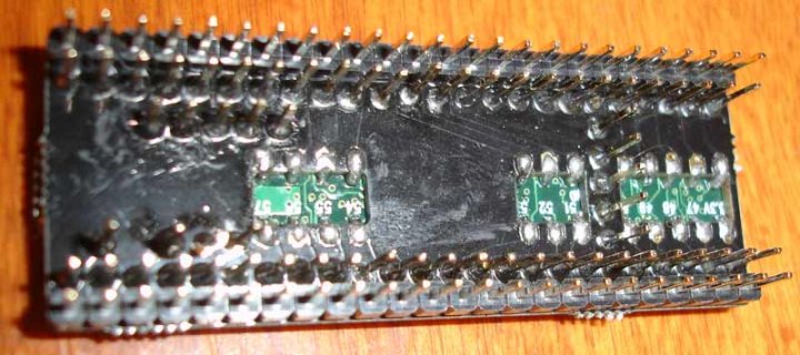
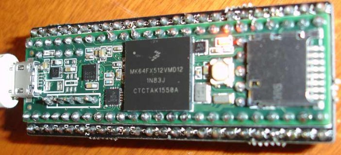
So I went ahead and built one, with the way Frank showed. That is I soldered most of the pins to the top of the Teensy side, then pulled off the spacers on the bottom. This can be a real pain in the ... I helped myself by using smaller sections (like 8 pins each), so only had to work 8 off at a time.

The issue on this one is that for example with inner pins, it is hard to pull this many spacers off and leave all of the pins perfectly aligned, such that you can then get the castellated adapter board over all of the pins. I finally did by getting most of one side in, then using small screwdriver, get each misaligned pin in place until all were in place. Then a bunch more soldering...

T3.5-castellated-bottom.jpg

T3.5-castellated-top.jpg

Note, I did not separate VIN from USB and needless to say won't be able to now.

I have not yet tested all of the connectivity, but assuming they all work, I can cut out all of the interior pins as I have duplicates on the outer row. So far I have only downloaded blink to this board to verify I had not totally screwed it up.

So again this is doable. Will see if I think I wish to now integrate this into some board design or not.

Kurt

Update: ran sketch to verify I could talk to different pins. So far verified, I can talk to 40-57
 
Last edited:
Blinking is a good start. And you can still get to the button.

I have a set of those coming - hopefully it tests out to get it all working with the inside pads coming out cleanly.

Too many pins to solder - so many options to pick ... starting with cutting the vin trace . . .
 
Yes - As I sort of mentioned in the update above, I also downloaded program, that can blink any pin, you enter the pin number. and it starts blinking that pin. If the pin is #13, it blinks it, else it puts pin 13 into input mode. This allows me then to use jumper from 13 to the pin I choose and if it is working the LED will blink... As I mentioned it worked for all of the surface mount pins.

As you mentioned, I still have access to the program button, also have pins on outer row for both PGM and RST, which I have manually tied to ground and it appears like they are working as well.

Again not sure where I will use this. Could for example try to modify my simple flexboard with LoRa, But adding another two rows of pins does make things tight!

Maybe now start playing with building my main board of this thread!
 
Status
Not open for further replies.
Back
Top