Several questions about the Teensy 3.5 & 3.6 boards

Status
Not open for further replies.

loglow

Well-known member
Hi, I'm excited about the 3.5 and 3.6 and I'm almost finished with a breakout for them.
I have several questions about the boards though, so here goes...


A) USB host port power selection
A.png

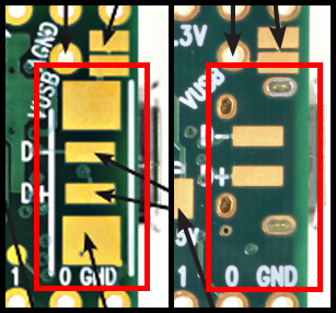
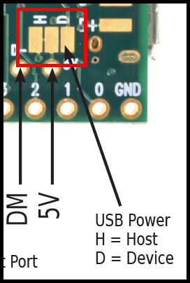
Regarding these USB power selection pads on the 3.6:

  • What is the intended use (procedure-wise) of these pads?
  • They appear to be intended to be used as a sort of solder jumper, is this correct?
  • Presumably, the host device (Teensy) is providing power by default, is this correct?
  • Does the trace between the H pad and the center pad need to be cut in order to change the setting?
  • My understanding is that these pads serve no purpose whatsoever on the 3.5, is this correct?

B) USB host port ID pin

B.png

Along the same lines as above, I'm wondering about the USB ID value of the USB host port (on the 3.6) and this pin in particular:

  • The pin is marked as GND on the info card, indicating that the port is indeed configured to be a host port, correct (slave would be floating)?
  • However, if the USB power setting is changed (see question A above) does this pin still remain grounded?
  • Basically, in that case, does this port remain a host port but no longer provides any power to the connected device?
  • Or does the connected device then become the Host (and this pin would have to become floating, I believe)?
I'm no expert regarding USB (OTG/master/slave config, etc.) so hopefully someone can help shed some light on this.


C) Debug pins and the G pad

C.png

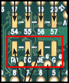
  • I'm 99% sure that this pad marked with a G is just another ground connection, am I correct?
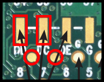
  • Also, I understand that the DD, DC, and DE pins are for debugging, but what protocol are these signals?

D) Onboard USB port in host mode

D.png

The pads for a USB host-mode 150uF cap were removed on the 3.5 and 3.6...

  • Is this because the 3.6 has a dedicated USB host port?
  • Or is it because the new USB connector has some through-hole mounting (which gets in the way)?
  • What if folks want to use 2 USB host ports?
  • Is the hardware still capable of allowing the onboard USB port to be put into host mode?
  • And if so, would one need to use a 150uF cap between GND and VUSB (as before)?
  • How about on the 3.5? Any differences from the 3.6?

E) Unused 3.5 connection point

E.png

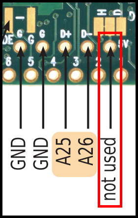
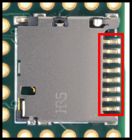
  • Is this pin on the 3.5 connected to anything at all?
  • Or is it disconnected/isolated/floating/grounded?

Thanks so much in advance for any help and/or clarification!
Have a wonderful night :)
 
Many questions... let's see if I can get a few answered quickly...

What is the intended use (procedure-wise) of these pads?
They appear to be intended to be used as a sort of solder jumper, is this correct?
Presumably, the host device (Teensy) is providing power by default, is this correct?

By default, the 2nd USB port power is configured for host mode, where Teensy sends power to a USB device.

[*]Does the trace between the H pad and the center pad need to be cut in order to change the setting?

Correct. The idea is you can cut apart the H pads and join the D pads, to configure where Teensy receives power.

My understanding is that these pads serve no purpose whatsoever on the 3.5, is this correct?

Also correct. There's no 2nd USB port on Teensy 3.5. The H pad connects to the unused 6 pin chip, so it does nothing. The D pad connects to an analog input pin which is not 5V tolerant, so it must not be used.

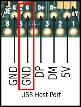
Along the same lines as above, I'm wondering about the USB ID value of the USB host port (on the 3.6) and this pin in particular:

That's not meant to be the USB ID pin (for USB On The Go).

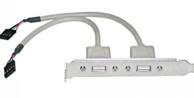
The intention is compatibility with these commonly available "internal PC" cables.

usbhost.jpg

The 5 pins are: Shield, Ground, D+, D-, 5V.

When/if software support for USB device mode on this port happens, we'll probably need get a similar cable made for this 5 pin socket to a panel mount USB B-type connector. While the hardware can do either host or device, it doesn't really support OTG. If you read Freescale's reference manual, you will find some mentions of the ID pin and OTG, but it's leftover info from generic documentation. This particular chip doesn't support the ID pin not OTG on this port. Even if it did, odds of anyone ever writing a library to support it would be slim.

The idea is you know which library you used in your program (today, neither exists) and you connect the corresponding cable to those 5 pins.


[/B] Debug pins and the G pad[/SIZE]
I'm 99% sure that this pad marked with a G is just another ground connection, am I correct?

Yes, it's ground.

Also, I understand that the DD, DC, and DE pins are for debugging, but what protocol are these signals?

DD is debug data (also called SWDIO) and DC is debug clock (also called SWDCLK). DE is an enable pin, which currently isn't supported. But future versions will tri-state DD & DC when DE is pulled low.

The pads for a USB host-mode 150uF cap were removed on the 3.5 and 3.6...
[*]Is this because the 3.6 has a dedicated USB host port?

Yes, and it has a 100 uF capacitor.

[*]What if folks want to use 2 USB host ports?

It's hard to imagine why you'd want a second USB host port at 12 MBit/sec when you could just connect a USB hub to the 480 Mbit/sec port. But if you *really* want to do this, and if you want to do it with a weak 5V power supply (not enough to supply USB hot plugging), you'll have to add extra capacitance in parallel with your 5V power source.

[*]Is the hardware still capable of allowing the onboard USB port to be put into host mode?

Yes. But the connector is a USB Micro-B, not the Micro-AB used on Teensy 3.2, so you'd also need to deal with wiring the USB cable somehow.

[*]And if so, would one need to use a 150uF cap between GND and VUSB (as before)?
[*]How about on the 3.5? Any differences from the 3.6?

Look, you can ask a lot "what if" scenarios, but in practice, implementing USB host always requires some attention to your power supply and how you'll handle hot-plug events.

Teensy 3.6 has a (currently still undocumented) USB host current limit switching and 100 uF capacitor, which is intended to give you a pretty good start and have a good chance of things "just working" even when running from USB power over a cable from a PC. I'm planning to write more about this in a couple weeks. Maybe best to wait for that? The update with hardware details will come long before working library code to really support this new hardware.
 
Paul, thank you so much for your detailed and thoughtful (and extremely quick) reply. I appreciate it so much!

By default, the 2nd USB port power is configured for host mode, where Teensy sends power to a USB device.

When the 2nd USB port is configured into the (non-default) "Device" power setting (H-to-center trace cut & D-to-center pads shorted) what exactly happens?
Does the state of the 5V pin change? Or some other internal logic?

The D pad [on the 3.5] connects to an analog input pin which is not 5V tolerant, so it must not be used.

Could this D pad (on the 3.5) be used as an extra general purpose analog input (obviously without shorting it to the center pad)?
If that's possible (hardware-wise) is there any way to address the pin software-wise?
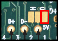
You mentioned the D and H pads, but what about the 5V hole/pad (on the 3.5)?

DD is debug data (also called SWDIO) and DC is debug clock (also called SWDCLK).

My understanding was that the 2 circular test points below the 3 debug pads were SWDIO (on the left) and SWCLK (on the right), is that also correct?
If so, is there any difference between the signals on the pads vs the test points (since they aren't visibly shorted to each other)?

Thanks again for all the info, and sorry about the question overload in my initial post :p
 
The unused USB pins can be used for ADC, and there is a modded file on the beta thread to support it, Don't believe it's in the official Teensy download given it's complex to explain the limits and use. Same as the mod to use the SD card pins as general IO if you somehow run out.
 
Actually they are supported (I added them awhile ago). Look at the back side of the T35 card:
attachment.php

As is shown in the Beta thread and you will See A25 and A26.

But as mentioned earlier and on the card: These pins like A10, A11... Are not +5v tolerant.
 
Same as the mod to use the SD card pins as general IO if you somehow run out.

C.png

Cool. I assume by soldering right onto these pins? Can you point me to the info about this?

Look at the back side of the T35 card: As is shown in the Beta thread and you will See A25 and A26.

A.png

Thanks for the info about A25/A26, but I was more wondering about the "D pad" (above and to the right of the 5V hole) since Paul said:

The D pad connects to an analog input pin which is not 5V tolerant

B.png

I'm also still wondering about the difference between the DD/DC pads and the test points below them.
Checked with a meter and none of them are shorted to each other.
 
Someone (KURTE??) made a board that fits into the sd-slot. It is a kind of SD->pinheader adapter. I have some of them, they work good. It must be somewhere in this forum..
Hint: Tell OSH.Park to use a 0.8mm PCB.
 
I'm also still wondering about the difference between the DD/DC pads and the test points below them.
Checked with a meter and none of them are shorted to each other.

Replying to myself here :p
Here's my thought: DD/DC pads are SWD for the main processor, and the 2 test points are SWD for the bootloader?
So they're both SWDIO/SWCLK signals, but for 2 different chips?
 
It was noted there are exposed 'factory test points' it seems used to program the bootloader chip. They are not for end use - if you manage to do anything intelligible on them - you will just brick your Teensy bootloader.
 
Someone (KURTE??) made a board that fits into the sd-slot. It is a kind of SD->pinheader adapter. I have some of them, they work good. It must be somewhere in this forum..
Hint: Tell OSH.Park to use a 0.8mm PCB.

Yes - I have played around with these as you can see in the post: https://forum.pjrc.com/threads/34808-K66-Beta-Test?p=110261&viewfull=1#post110261

The files are up on github in: https://github.com/KurtE/Teensy3.1-Breakout-Boards/tree/master/microsd-Adapter
That directory has the diptrace design files as well as the zip file with gerber files that should work at a few of the fabricators. This time I used Seedstudio as SD cards are about .75mm. So I ordered the .6mm from Seeed. the .8mm might fit directly or you might need to sand it down. Note: no etch on the one side...
 
It was noted there are exposed 'factory test points' it seems used to program the bootloader chip. They are not for end use - if you manage to do anything intelligible on them - you will just brick your Teensy bootloader.

Yeah. I was having a brain fart and getting all confused about DD/DC being SWDIO/SWCLK and then the test points ALSO being SWDIO/SWCLK--and of course they both are--but for two different chips. At least that's what makes the most sense to me right now, until someone can confirm this to be the case.
 
loglow - it was confirmed on your other 'Test Points' thread:

Indeed, don't mess with those test points. The protocol is very complex, so the odds of doing anything by mistake are slim. But if you do, the only likely outcome is bricking your Teensy. Don't do that.
 
the SD card pins are described in
https://forum.pjrc.com/threads/34808-K66-Beta-Test?p=106730&highlight=sdio#post106730
and defined in core_pins.h. The K66 beta test thread also describes several PCB breakouts to insert into the micro-SD slot and breakout the pins, or you could solder....

Thanks very much for the link and info. Clever idea.

Someone (KURTE??) made a board that fits into the sd-slot. It is a kind of SD->pinheader adapter. I have some of them, they work good. It must be somewhere in this forum..
Hint: Tell OSH.Park to use a 0.8mm PCB.

Glad to hear they work well. Going to try and make one of these.

Oh - I saw Paul had an SD-slot adapter already on OSH - came up under his name on projects.

Found it. For anyone else interested, here's the link: https://www.oshpark.com/shared_projects/FdwGV8nO

Yes - I have played around with these as you can see in the post: https://forum.pjrc.com/threads/34808-K66-Beta-Test?p=110261&viewfull=1#post110261

Awesome. KurtE, have you had good success with this adapter board? Does it fit well and function reliably?

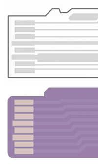
sd.png

I noticed that yours has the little cutout/notch shape versus Paul's which has a more simplified edge profile. I wonder how that affects the fit?
 
You're absolutely right...
:) - to extend an adage : Rolling stones gather no moss ... and they don't take direction well either.

I had some of Kurt's made by PCBS.io - their 1.2mm stock took a lot of work to file down - I got it to fit and got distracted so I never actually wired it up. The socket on the Teensy doesn't have the latch mechanism as I saw it - so that tooth is perhaps extraneous - expect the OSH cut on Paul's is probably just as well. Paul mentioned some detail about the router bit size and was happy with the result he got.
 
I noticed that yours has the little cutout/notch shape versus Paul's which has a more simplified edge profile. I wonder how that affects the fit?

It slides out more easily. The notch helps keep the card in the socket.

Mine was designed for the test fixture, to plug in during the testing for the board, so the intention was to *not* have the notch.
 
Awesome. KurtE, have you had good success with this adapter board? Does it fit well and function reliably?
It worked for me.

I did this to work with the original Beta board. So far I only populated one of these. With it I was able to hookup an ILI9341 display, which is nice as the SD card pins have 3 CS pins for the SPI buss, so was able to use SPI for both CS and DC. I was then able to use my hacked up version of the ILI9341_t3 library that works on all SPI busses and also works even when there is only 1 hardware CS pin. It is sort of nice to be able to temporarily add a display to the board...

I have also tried it on the production board and it still works. Paul already mentioned about the notch. Don't know how much it helps, but it does appear to hold in pretty well. Now that I have production boards, if/when I make new ones, I would probably make some changes. That is I would probably shorten the neck. At the time I did not know if the Teensy would have spring loaded SD card holders, that you had to leave room for to push in to release... Nope: so can shorten. Also I would probably convert from having all the pins in a row, to two rows of pins, to make it easier to fit on some of my boards I am now playing with.
 
Many questions... let's see if I can get a few answered quickly...
The intention is compatibility with these commonly available "internal PC" cables.

View attachment 8472

The 5 pins are: Shield, Ground, D+, D-, 5V.

Ah, I was wondering about this: the second ground is for the shield, then!

Just from a quick online search on the matter, I've come across different opinions as to whether the shield should be grounded or not, but no definitive answer. Your recommendation is that we do ground it, then?
 
Status
Not open for further replies.
Back
Top