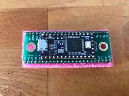
Preview of 3.5 & 3.6 Breakout boards -- Feedback welcome!

Status
Not open for further replies.

loglow

Well-known member
Heya, I've been working on some general-purpose Teensy 3.5 & 3.6 breakouts, since folks have really seemed to like these for the 3.0, 3.1, & 3.2.

I'm getting ready to finalize them, and I thought I'd share them on here and solicit some feedback!
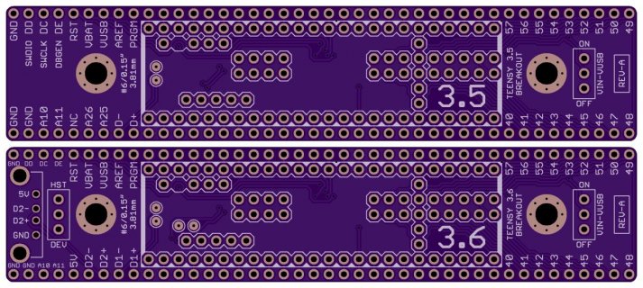
T35_T36_preview.jpg
(click for full-size image)

Some notes:

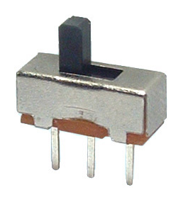
The 3-pin rectangles are for SPDT switches, like these:
spdt.png

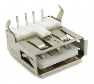
The 3.6 version allows for mounting a full-size female USB A jack, like these:
usba.png

RST = shortened version of RESET
HST/DEV switch = select power mode for the USB host port
D+/D- = T3.5 onboard USB port data lines (since the 3.5 only has 1 USB port)
D1+/D1- = T3.6 onboard USB port data lines
D2+/D2- = T3.6 secondary USB host port data lines

I debated adding pads for a 150 uF cap to put the onboard USB port into host mode, but eventually decided against it because:
  1. those who need USB host will get a 3.6 and use the secondary USB port, and
  2. the onboard USB jack changed from Micro-AB to Micro-B so you couldn't even use a USB OTG adapter
I also debated breaking out the 2 test points (below the DD/DC/DE pads) but also (probably) decided against it because:
  1. hacking the (closed-source) bootloader doesn't seem like such a useful/fun activity for the vast majority of people
  2. it would add 2 pogo pins to the BOM as an unnecessary expense or an annoying option to keep track of
  3. Paul said messing with those pins was a bad idea and would probably brick the Teensy
(The remnants of the test point breakouts are the extra GND points in the lower left corner. Couldn't quite bring myself to shorten the board by 0.1" though, for the sake of symmetry)

Still kind of debating what to do with the "not used" 5V pin on the 3.5 breakout, which is currently marked NC. Trying to figure if it could be useful for anything at all... if not, it might become another GND?

Also debated making just 1 board for both the 3.5 and the 3.6 since they're so similar, but I think I've decided against it for the sake of clarity. It's really annoying to try and distill information like: "if you're using a Teensy 3.5, this pin is A25, but if you're using a Teensy 3.6, it's the USB host port's D+ line" into such a tiny amount of silkscreen space. I'm still kind of waffling on this decision though.

Anyway, let me know what you think :) Happy to answer any questions, and thanks!
 
Last edited:
Heya, I've been working on some general-purpose Teensy 3.5 & 3.6 breakouts, since folks have really seemed to like these for the 3.0, 3.1, & 3.2.

I'm getting ready to finalize them, and I thought I'd share them on here and solicit some feedback!

View attachment 8489
(click for full-size image)

Some notes:

The 3-pin rectangles are for SPDT switches, like these:
View attachment 8487

The 3.6 version allows for mounting a full-size female USB A jack, like these:
View attachment 8488

RST = shortened version of RESET
HST/DEV switch = select power mode for the USB host port
D+/D- = T3.5 onboard USB port data lines (since the 3.5 only has 1 USB port)
D1+/D1- = T3.6 onboard USB port data lines
D2+/D2- = T3.6 secondary USB host port data lines

I debated adding pads for a 150 uF cap to put the onboard USB port into host mode, but eventually decided against it because:
  1. those who need USB host will get a 3.6 and use the secondary USB port, and
  2. the onboard USB jack changed from Micro-AB to Micro-B so you couldn't even use a USB OTG adapter
I also debated breaking out the 2 test points (below the DD/DC/DE pads) but also (probably) decided against it because:
  1. hacking the (closed-source) bootloader doesn't seem like such a useful/fun activity for the vast majority of people
  2. it would add 2 pogo pins to the BOM as an unnecessary expense or an annoying option to keep track of
  3. Paul said messing with those pins was a bad idea and would probably brick the Teensy
(The remnants of the test point breakouts are the extra GND points in the lower left corner. Couldn't quite bring myself to shorten the board by 0.1" though, for the sake of symmetry)

Still kind of debating what to do with the "not used" 5V pin on the 3.5 breakout, which is currently marked NC. Trying to figure if it could be useful for anything at all... if not, it might become another GND?

Also debated making just 1 board for both the 3.5 and the 3.6 since they're so similar, but I think I've decided against it for the sake of clarity. It's really annoying to try and distill information like: "if you're using a Teensy 3.5, this pin is A25, but if you're using a Teensy 3.6, it's the USB host port's D+ line" into such a tiny amount of silkscreen space. I'm still kind of waffling on this decision though.

Anyway, let me know what you think :) Happy to answer any questions, and thanks!

Hi, will this plug into a 64pin dil? If so how do i buy one for my 3.5?
Kind regards Baggey
 
good stuff. It would be easier to pass comment if the schematics for T3.5/3.6 were available but I don't think they've been published yet?

Meanwhile I've been thinking it would be nice if someone devised a breakout allowing t3.5/3.6 to drive/accept existing (3V3 based) shields in Arduino Uno / Mega format. Is this likely?
 
Last edited:
good stuff. It would be easier to pass comment if the schematics for T3.5/3.6 were available but I don't think they've been published yet?

I can't imagine tha the schematic is useful for you in this case.
I guess it will be pretty similar to one of teensy 3.2
 
I'm new to teensy = unfamiliar with teensy breakout culture, but have a few comments/questions FWIW:

The back side of the 'Welcome to Teensy 3.5 card' shows A25 = D+ and A26 = D- so maybe duplicating those pins on the breakout is overkill ?

The back side of the 'Welcome to Teensy 3.6 card' shows DP = D+ and DM = D-.
I guess DP means D Plus and DM means D Minus? but I can't find D1+/- or D2+/- anywhere on the card?

I'm curious: how would one normally connect/wire/solder the pads on the back side of the teensy to the matching holes you've provided for receiving the T3.5/3.6 back-side ?
 
Last edited:
A couple of comments:

1) I would suggest reordering the top left pins to be:
  • DD
  • DC
  • DE
  • AREF
  • Reset
  • Program
  • VUSB
  • Ground

The reason is to group VUSB, Ground, and the VIN pin next to each other to allow for easy connection to combined battery/chargers. In particular, the Adafruit Pro Trinket Lilion/Lipoly Backpack Add-on (https://www.adafruit.com/products/2124) uses that pinout, but others like onehorse's charger do need the VIN, VUSB, and ground pins. Or alternatively, having the Reset, Program pins near a ground pin makes it easier to bring them out to add an external reset/program button.

2) I don't know if a 4.2" board pushes the prices much higher than a 4" board, but if it does obviously you have to consider whether the extra cost is worth it. You didn't mention whether the board was going to be available for sale or available for download. If it is in the download category, and you anticipate other people hacking on it, the 4.2" size means you cannot use the free version of Eagle. And on the commercial Eagle side, you would have to have a premium license ($820) compared to the standard license ($69).

3) I haven't measured it, but I wonder if the VIN/VUSB pins are too close to the mounting holes, particularly if you use standard screws and a on-on switch like you mention. I've had some projects where the only way I could attach a spacer is to get nylon screws/nuts, and use diagonal cutters to reduce one side.

4) From the pcb, it looks like the way you attach the bottom pins is by soldering a 2x9 SMT header to the bottom of the Teensy. As somebody whose soldering skills are somewhat basic, I have been hesitant to solder such headers on to the Teensy, because it is hard to get it positioned just right. I find it easier to solder castellated boards to attach the bottom pins.

5) With the 3.6 board, I would be worried that it may be too tight of a fit to attach a standard micro USB cable for programming over the secondary USB header, particularly if you use HST/DEV.

6) With either board, I wold wonder if I can get the micro SD card out if I attach an on-on switch to switch VIN/VUSB. Similarly for a screw mounted in the mounting hole, but I imagine you can remove the screw if necessary.
 
good stuff. It would be easier to pass comment if the schematics for T3.5/3.6 were available but I don't think they've been published yet?

Meanwhile I've been thinking it would be nice if someone devised a breakout allowing t3.5/3.6 to drive/accept existing (3V3 based) shields in Arduino Uno / Mega format. Is this likely?

The existing 3.2 -> Arduino shields can be used, providing you use use wires to connect the DAC0 (pin 21), Program, Reset, and Vbattery pins from their 3.6 location to their 3.2 location. Here are some of the 3.2 boards:
 
thanks for those clues MichaelM ... I think I'll grab a couple of those Sparkfun shields
 
Last edited:
This may be a silly question, but does bottom side of the USB cable plugged into the Teensy have enough clearance to not touch the switch or host connector?
 
Thanks for the comments and questions so far. :)

will this plug into a 64pin dil?
These boards won't fit into a 64 pin DIP socket. They have 2 rows of 42 pins which are spaced 0.8" apart. That said, I'm looking into this idea...

If so how do i buy one for my 3.5?
When the design is finalized, it'll be available on Tindie.

I've been thinking it would be nice if someone devised a breakout allowing t3.5/3.6 to drive/accept existing (3V3 based) shields in Arduino Uno / Mega format. Is this likely?
I'm working on this exact thing. More info soon...

The back side of the 'Welcome to Teensy 3.5 card' shows A25 = D+ and A26 = D- so maybe duplicating those pins on the breakout is overkill ?
The Teensy 3.5 and 3.6 use the same PCB, so the A25/A26 pins on the 3.5 are marked with the functions of those same pins on the 3.6 (which are D+/D- for the USB host port). The pins aren't duplicated: the D+/D- pins on the 3.5 breakout are for the onboard USB port, not the extra host port. It is a little confusing, marking-wise, to have different pairs of signals on the Teensy both marked with D+/D-, but they're actually for two different USB ports. Hope this makes some sense. :p

The back side of the 'Welcome to Teensy 3.6 card' shows DP = D+ and DM = D-. I guess DP means D Plus and DM means D Minus?
Yeah, I've seen +/- signals also indicated with P/N (positive/negative) or P/M (plus/minus).

I can't find D1+/- or D2+/- anywhere on the card?
The reason I went with D1+/- and D2+/- is to differentiate between the two USB ports on the 3.6. D1 is the onboard USB port and D2 is the extra USB host port.

I'm curious: how would one normally connect/wire/solder the pads on the back side of the teensy to the matching holes you've provided for receiving the T3.5/3.6 back-side ?
They're connected using standard double-row surface-mount 0.1" pin headers.

I would suggest reordering the top left pins
These are good points. I've reordered them to be: DD, DC, DE, AREF, VBAT, RST, PRGM, VUSB, GND

I don't know if a 4.2" board pushes the prices much higher than a 4" board, but if it does obviously you have to consider whether the extra cost is worth it.
A difference of 0.18 square-inches makes very little difference in cost. At OSH Park that would be a $0.30 difference.

You didn't mention whether the board was going to be available for sale or available for download.
These boards will be available for sale on Tindie. Not sure of exact cost but it'll be comparable to my existing 3.2 boards (which are $8 PCB / $12 kit). Not putting a link here because I don't want to be perceived as advertising inside this thread.

I wonder if the VIN/VUSB pins are too close to the mounting holes
The holes are designed for use with #6 pan-head machine screws, and the head sits entirely inside the plated area. A standard #6 spacer has an OD (outer diameter) of 1/4" I believe, which would also fall entirely within the plated area.

As somebody whose soldering skills are somewhat basic, I have been hesitant to solder such headers on to the Teensy, because it is hard to get it positioned just right.
They aren't bad with a little practice. Flux applied to the pads first helps. I usually tape the board in place, put the header on, then use a second piece of tape to hold the header in place, just on one edge of it, while I tack a few pins. The alignment doesn't have to be crazy dead-on, just close enough.

With the 3.6 board, I would be worried that it may be too tight of a fit to attach a standard micro USB cable for programming over the secondary USB header, particularly if you use HST/DEV.
This is an excellent point, and I'm investigating it. I'm actually leaning toward using a micro-AB jack instead of the full-size A jack, which would also reduce the height.

With either board, I wold wonder if I can get the micro SD card out if I attach an on-on switch to switch VIN/VUSB. Similarly for a screw mounted in the mounting hole, but I imagine you can remove the screw if necessary.
The screw definitely won't be a problem, but the switch could be. I'm looking into this. Thanks for the heads-up.

This may be a silly question, but does bottom side of the USB cable plugged into the Teensy have enough clearance to not touch the switch or host connector?
Not a silly question at all, totally depends on the height of the switch's actuator! MichaelMeissner pointed this out too. I'm investigating it and might need to make some changes.

The http://embeddedcoolness.com/shop/rfx...ping-area-kit/ works with the 3.5/3.6. and all UNO pins are accessible.
Your link didn't work, but this one does: http://embeddedcoolness.com/shop/rfx-teensy3-x-nrf24l01-carrier-board-w-prototyping-area-kit/
 
So here's something a little different, inspired by the DIP-64 idea and clearance issues.

Here's my idea for a Teensy 3.5/3.6 to DIP-64 form-factor breakout.

dip64.jpg

It's 3.2" x 1" (with standard 0.9" row spacing) and would fit right into a DIP-64 socket or a breadboard. Instead of putting every pin on two rows, it puts (nearly) every I/O pin onto two rows, and focuses on breaking out all the bottom pins. (I say "nearly" because A25/A26 aren't on the outer rows, but they're easy to get at on the USB host header). This could be assembled with extra-long pin headers on the three internal 1x5 pin sections for easy hookups to ribbon cables.

Anyway, this would be kind of a "compromise" board. Not necessarily a replacement for the ones above. With a 3.5, you'd just leave off the USB jack and bottom switch. Still a little concerned about the USB jack clearance, so I'll have to verify that...maybe a board-cutout jack would solve that?

Let me know what you think!
 
It's good you downsized the USB port, like most I hardly have any type A ports / cables left these days.

You're maybe thinking of providing two options: one a bare board, the other with all the headers and USB connectors etc bundled, including switches and those "standard double-row surface-mount 0.1" pin headers"

Regarding the various USB ports, where are you finding that information ? (note I didn't mention the elusive T3.5 / 3.6 schematics :) )
 
Last edited:
It would be helpful to include "standard double-row surface-mount 0.1" pin headers" with the product.
They certainly will be included! In fact, headers are included in all my kits (both present and future) :)

Regarding the various USB ports, where are you finding that information ?
Combination of experience with previous Teensy boards, the pinout reference cards, and the helpful people on this forum.
 
...
Regarding the various USB ports, where are you finding that information ? (note I didn't mention the elusive T3.5 / 3.6 schematics :) )

I note you did mention the schematic again . . . as far as pin naming/function ... the ~3 month beta ran with 80+ boards shipped for testing and no schematics and no pictures allowed - and the first 8 boards only had selective bottom pins brought to unmarked holes. That K66 Beta thread has just pin #'s and info that likely covers everything - more info may have come out after the KS announcement.

The schematics always show up some short time after the product ships - and the last 3 new Teensy's didn't have the weeks of Kickstarter to force KS updates and production of 6000+ boards on day 1. The first preliminary Eagle Drawing showed up 2 months back on 8/20 - with refinements and two more in the next month for the 3 I have in that post #8.
 
thanks defragster. I do understand we're still on the 'bleeding edge', although it may start to settle soon. It's totally understandable given the amazing efficiency of the pjrc crew in delivering on the KS, and to such a high standard already.

There's an amazing amount of information on this site, a credit to all in the inner circle. It can take me a while to find things, and sometimes I can't be sure the configuration info I find matches as my KS hardware. Not that I really mind. I've visited your post#8 a few times and I pilferred lots of good stuff from it.
 
ports, where are you finding that information ? (note I didn't mention the elusive T3.5 / 3.6 schematics :) )
Actually you just did! ;)

As already mentioned, those of us who got the early beta boards had very little information, but it was enough to deduce a lot of the details. As mentioned earlier, we were able to deduce a lot of the information, by looking at the first code Paul released to the beta for the boards, plus a lot of searching through the reference manuals. Note: earlier in the beta posting #3 was updated as information was found.

As I mentioned in the #3, the PDF that I keep referring to: K66 Reference Manual I refer to a lot! From figuring out what Arduino pin maps to which K66 pin from the file:
C:\arduino-1.6.12\hardware\teensy\avr\cores\teensy3\core_pins.h (your location will likely be different) starting at about line 129. From this we were able to deduce pin 0 is B16

Now if you go to the PDF I mentioned to section 11.3, you will see the K66 Signal Multiplexing and Pin Assignments table. If you then search for B16, you will find PTB16 which is the pin and you will find what are all the different ways this pin can be configured: Yes sometimes the names are somewhat Cryptic.
Code:
95 E10 PTB16 TSI0_CH9 TSI0_CH9 PTB16 SPI1_SOUT UART0_RX FTM_CLKIN0 FB_AD17/SDRAM_D17 EWM_IN TPM_CLKIN0
From this you will see mode(ALT) 3 is UART0_RX, which is used for Serial1 RX pin.

Now if you repeat this, you can build a complete list of pins, which I did for the Excel Spreadsheet. I think one of the later ones was posted in
https://forum.pjrc.com/threads/34808-K66-Beta-Test?p=113651&viewfull=1#post113651

Note: for some of the later things that were deduced, like how the T3.5 does not have USB Host, but pins can be used as Analog, took a little more work. Basically you figure out that DP/DM map to K66 pins USB1_DP, which on the chip is PIN J1 and USB1_DM is chip pin K1 and then look at the K64 reference manual to see what are on those pins. For example you will find K1 and it has the capabilities (25 K1 J1 16 ADC1_DP1 ADC1_DP1 ADC1_DP1) Which shows it is an Analog only pin, so Added the mapping to the Pin table and Analog code...

Sorry if I am off topic...
 
So here's something a little different, inspired by the DIP-64 idea and clearance issues.

Here's my idea for a Teensy 3.5/3.6 to DIP-64 form-factor breakout.

View attachment 8507

It's 3.2" x 1" (with standard 0.9" row spacing) and would fit right into a DIP-64 socket or a breadboard. Instead of putting every pin on two rows, it puts (nearly) every I/O pin onto two rows, and focuses on breaking out all the bottom pins. (I say "nearly" because A25/A26 aren't on the outer rows, but they're easy to get at on the USB host header). This could be assembled with extra-long pin headers on the three internal 1x5 pin sections for easy hookups to ribbon cables.

Anyway, this would be kind of a "compromise" board. Not necessarily a replacement for the ones above. With a 3.5, you'd just leave off the USB jack and bottom switch. Still a little concerned about the USB jack clearance, so I'll have to verify that...maybe a board-cutout jack would solve that?

Let me know what you think!

When can i Buy?
 
Here's an image of a 3.2. Note Usb is still there? So the 3.5 will still have usb and sd socket.
s-l1600.jpg

This might work for the 3.6 as well. But theres no point its not 5V tollerant?


Kind regards Baggey
 
Here's an update for what I'm thinking of as the "standard" full-size breakout board (from my original post):

662905b4f2c8068c4ffac484a65a6298.jpg

Changes:
  • Uses a Micro-AB jack instead of full size USB-A
  • Shaved 0.2" off the board (2 pins on each side) mostly so one regular 40 pin header can be used per side. Did this by removing extra GNDs and putting A10/A11 where the "extra" GND and 3V3 are on the Teensy.
  • Changed width to 1" (was 0.9")
  • Moved switches so they won't interfere with the onboard USB or SD card
  • Decided to make just one board for both 3.5 and 3.6 since 5V/D2-/D2+ are really the only differences.
  • Reordered upper-left pins as per suggestion, except AREF(ARF) and VBAT(VBT) moved to other side.
  • FYI: VU = VUSB, AG = AGND (no space for more letters!)
  • Had a lot of internal space left over on the right side, so I added a 25 pin (5x5) protoboard area + 2x 4 pin rails for 3V3 & GND.
  • Mounting holes are 2.8" apart now (they were 3")
TODO: Still need to verify USB jack/connection clearance & fit.

Leaning towards making both this & the DIP-64 variant.

The feedback has been super helpful. Thanks so much. Any additional comments are more than welcome! :D

PS. Also been working on an Arduino Mega/Due form-factor adapter board for fun...
 
When can i Buy?
When the designs are finalized and the boards are manufactured :) Should be within a couple weeks.

Here's an image of a 3.2. Note Usb is still there? So the 3.5 will still have usb and sd socket. This might work for the 3.6 as well. But theres no point its not 5V tollerant?
Sorry, but I'm not quite following what you're asking here. Can you try rephrasing your questions?
 
Status
Not open for further replies.
Back
Top