Preview of 3.5 & 3.6 Breakout boards -- Feedback welcome!

Status
Not open for further replies.
@loglow - saw a post tonight 'had to settle for a T_3.5 as the T_3.6 was out of stock'.
The PJRC store tonight showed the T_3.6 stock is "Low", not so for the T-3.5.
 
When the designs are finalized and the boards are manufactured :) Should be within a couple weeks.


Sorry, but I'm not quite following what you're asking here. Can you try rephrasing your questions?

What im trying to say is. The 3.5 just needs pins soldered on to it. Then it plugs into the pcb you make. We then solder that to that. Leaving the teensy intact with original usb and SD socket.

It can then be used on breadboards or on single sided PCB's with either a 64 Pin socket or ZIF Type. Im interested in the 3.5 Because its 5v tolerant making useful for retro interfacing.

I dont know why they make the device like they do, when they could of made it with access to all pins anyway.

If you decide to make the 64 Pin variant i want two of them or if you only make a small batch put me down for two!

Kind regards Baggey
 
Looks like a nice board. If I were to purchase some, I would be more likely to use your DIP-64 version on a breadboard, which would be a nice setup to try out things.

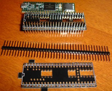
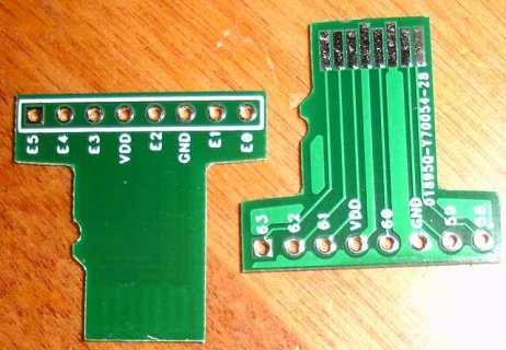
I have also been wondering if I should have made my Castellated adapter board:
T3.6-castellated-parts.jpg
Look more like what you have, where you bring out all of the new pins to the ends, instead of to the 2nd row of pins.

The problem I was finding though was even with my adapter board, that only increases the width to .9" and left the length alone, I found I did not want to incorporate it into my main boards as it used up a lot of room, especially for boards that I want some specific form factor, such as the size of the touch display or RPI form factor. Example my maybe simpler version of Franks flexboard which uses LoRa instead of wifi.

My issues of adding to the length is, suppose I wish to use my board inside of a case. Example the sudo-flexboard which is the size of the Touch screen that PJRC sells. Suppose I wish to build the case which gives me a slot to slide in an SDCard. Having pins on the right hand side would probably interfere with that layout. Also if I mount anything in those pins, would need to make sure there is clearance to install and remove SDCards. Or if I wish to mount the board, on an edge to give access to the Teensy USB connector, adding stuff to the left hand side might be problematic.

So I am sort of at an impasse with myself on what would be the best approach.

Again great looking board, when they are available my have to pick up a few to try them out on breadboard.

Kurt
 
The existing 3.2 -> Arduino shields can be used, providing you use use wires to connect the DAC0 (pin 21), Program, Reset, and Vbattery pins from their 3.6 location to their 3.2 location.

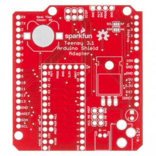
@MichaelM, I'm wiring up the SFE T3.1 adapter (https://www.sparkfun.com/products/13288). I guess I should wire the T3.5 / T3.6 DAC0 (pin A21) to A14/DAC on the adapter, as that's only connected to JP8. Is that what you meant?

SFE t3.1 adapter - top.jpg
 
@MichaelM, I'm wiring up the SFE T3.1 adapter (https://www.sparkfun.com/products/13288). I guess I should wire the T3.5 / T3.6 DAC0 (pin A21) to A14/DAC on the adapter, as that's only connected to JP8. Is that what you meant?

You need to attach the DAC0 pin to the A14/DAC pin in the shield (which is the back row on the Teensy 3.2) if you want the DAC to be available on the back row of pins. If you don't need to use the DAC (mostly to make sounds if fed through an amplifier), you don't need to connect that pin. The DAC is not one of the classic Arduino pins.

You need to connect the Program pin on the 3.6 to the prog pin on the shield if you want to access it in the back pins. If not, you don't need to connect it, but it can be problematical to force the Teensy into programming mode if a shield covers the Teensy.

If you plan to power the real time clock with a coin battery, you will need to connect the Vbat pins. Note, the position of the coin cell battery and ICSP header might be problematical for the 3.6, since the 3.6 would overhang these, and make them hard to use.

If you are not planning on using any of those features, you don't need to connect those pins.

There is this board that will help interconnect the pins (I have an order in, but it is still in the fabrication stage): https://pcbs.io/share/8gXO3.
 
No idea if its too late to add suggestions to this thread, but it would be nice to arrange the SWD debug pins a little better.

At least put DE next to GND for easier shorting to ground. It would be great to see a 2-pin header on the board, so you can put a jumper on it to short them out without the need to short them inside the debug cable.

Even better would be if you could put a full 9-pin or 19-pin 1.27 pitch debug header with the standard ARM pinout. So you could connect any jtag/swd tool with standard cables.
i.e. the smaller end of this sort of thing
https://www.olimex.com/Products/ARM/JTAG/ARM-JTAG-20-10/
 
I don't know if ideas are still being accepted, but it sure would be nice to be able to (optionally) mount an external VRef for the ADCs. I am not sure where it would sit on the board or how it can be integrated with the AREF pin so as not to clash when internal AREF is being used (1.2V or 3.3V), but it is a necessity for my projects, because the internal 1.2 REF is junk.

I can post a sample part number, but a quality external 3.3V voltage reference (the highest voltage allowed) with a low tempco (with perhaps some tiny 0.1 uF bypass caps to reduce noise) would be ideal, allowing for the full capability of the 16-bit ADCs.

BTW: The DIP-64 form factor is definitely a good move!
 
Last edited:
I have also been wondering if I should have made my Castellated adapter board:
I really like the idea of this, since it simplifies soldering, though at the expense of the test points. I experimented with surface mounting by putting through holes over pads, but I couldn't get reliable solder connections that way. The castellated edges also require a heat gun to remove.

No idea if its too late to add suggestions to this thread, but it would be nice to arrange the SWD debug pins a little better. At least put DE next to GND for easier shorting to ground. It would be great to see a 2-pin header on the board, so you can put a jumper on it to short them out without the need to short them inside the debug cable. Even better would be if you could put a full 9-pin or 19-pin 1.27 pitch debug header with the standard ARM pinout. So you could connect any jtag/swd tool with standard cables.
Not too late, and thanks for the suggestions. I can easily move DE next to GND on the DIP-64 version.

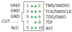
ARM-JTAG-20-10.png

I'm interested in this standard header, but I have some pinout questions:

  1. 3V3
  2. DD
  3. GND
  4. DC
  5. GND
  6. What goes here?
  7. Does this position require a removed pin?
  8. What goes here?
  9. NC
  10. RESET (Or should this be DE?)

I don't know if ideas are still being accepted, but it sure would be nice to be able to (optionally) mount an external VRef for the ADCs. I am not sure where it would sit on the board or how it can be integrated with the AREF pin so as not to clash when internal AREF is being used (1.2V or 3.3V), but it is a necessity for my projects, because the internal 1.2 REF is junk. I can post a sample part number, but a quality external 3.3V voltage reference (the highest voltage allowed) with a low tempco (with perhaps some tiny 0.1 uF bypass caps to reduce noise) would be ideal, allowing for the full capability of the 16-bit ADCs.

Cool, please post some part refs so I can checkout the footprints. There's plenty of room for SMD stuff and some room on the larger breakout for PTH stuff instead of the "proto" area. Don't think I'd want to go any smaller than 805 for SMD caps. I've never used one of these, so let me know if anything strange would need to happen re: schematic/hookup/connections.
 
Another round of updates to various boards, and some new ones! Getting closer to finalizing some of these. Feedback still welcome :D but ordering test boards very soon

DIP-64

1186b5ccf5d9ffaff6ad8b0cb9e97c39.jpg

  • Slightly more logical pin layout--the additional pins are now fully sequential counter-clockwise
  • Removed the USB micro jack--there wasn't really physical room for it, and it'd have been very annoying to hand-solder
  • Reordered SWD pins--as per suggestion by mundungus, DE is now next to GND
  • Changed markings of SWD pins--to stay consistent with the Teensy cards (DE, DD, DC)
  • Added orientation cutout--Just for the fun of it, I mean, it's DIP form factor after all...
  • Might be finished?

Standard

893bb83109f72cc63b6215aae45270d9.jpg

  • Also new slightly different pin layout--Teensy centered, moved some digital pins and A10/A11, VBAT, and AREF
  • Changed mounting hole locations--They now have 2.9" spacing, no longer symmetrical, due to other layout changes
  • Went back to full-size USB jack--Much much easier to solder, no need for an OTG adapter, should have room with onboard USB if using any right-angle micro-USB cable, but I still need to verify this with test cables & boards (once they've been made)
  • Moved switch locations--To make room for the USB jack and to stay consistent with the DIP-64 board
  • Slightly smaller proto area--down to 20 pins, due to the other layout adjustments
  • Looking into JTAG header (see earlier posts)
  • Looking into AREF source (see earlier posts)

Arduino

0a1a578eb5f415c841cce53464175e4c.jpg

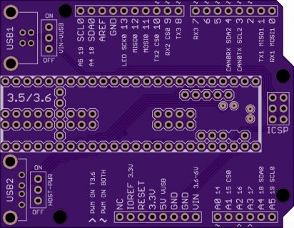
This is a new one, an Uno-sized (R3) adapter board. This is my first take on it. Powered via USB. Onboard USB is broken out to full-size USB-B jack, so blockage by the ICSP header isn't an issue, and the micro SD is easily accessible. T3.6 host port broken out to full-size USB-A jack. Switches same as other breakouts. Seems like there's plenty of room for other stuff being broken out into non-Arduino-standard headers--thoughts on this?

I'm also working on a Mega/Due-sized version, expanded from this one, but I don't have a draft finished yet.

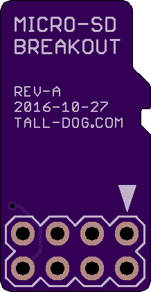
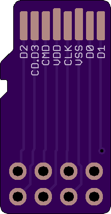
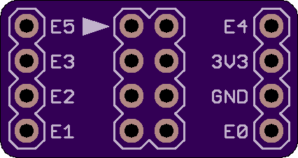
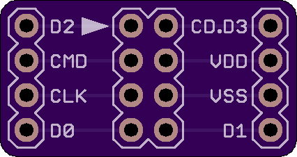
Micro SD Kit

7375aad1ee743510ba47c9f8205a2370.png 94ec38df4908c05146f459e681991733.png
79599b7ddf4a10591d4554d576b29584.png aefb4956d1671944b61e3ea2fc8f464b.png

Also new, and based partially on some previously discussed designs. Comes with two boards, designed to be attached to each other with an 8-pin ribbon cable (thinking 6" or 12"). The board that goes into the breadboard is designed so it can be flipped either way: one orientation shows the Teensy pins, the other shows the SD card pins--this decision needs to be made before soldering on the headers, since only the markings that end up on the "top" (exposed) side will be accurate. Played with using keyed/shrouded headers but decided they took up too much extra space.

Socket Kit

Planning to make a kit for any of the above boards to allow the Teensy to be socketed instead of permanently soldered. Would include all necessary female headers and alternate-size pogo pins, etc.
 
I don't know what it means for routing the signals, but if you had a vertical row where the Teensy 3.2 has its back row, and connect the DAC0, Program, 3.3v, Ground, and Vbat pins to their 3.2 location, it would allow mounting the prop shield underneath the 3.5/3.6 without using FrankB's shim board that does the same thing.
 
DIP 64 just like the layout of the 3.2 board but in 64 pin.

Please Keep the usb socket where it is and do away with the switches! Keep the design like your 3.2 Breakout board Plz.
Or when the PCB is produced Give the end user the option to use switches and move the USB or not have the switches and keep the USB where it is.

Kind Regards Baggey


Another round of updates to various boards, and some new ones! Getting closer to finalizing some of these. Feedback still welcome :D but ordering test boards very soon

DIP-64

View attachment 8645

  • Slightly more logical pin layout--the additional pins are now fully sequential counter-clockwise
  • Removed the USB micro jack--there wasn't really physical room for it, and it'd have been very annoying to hand-solder
  • Reordered SWD pins--as per suggestion by mundungus, DE is now next to GND
  • Changed markings of SWD pins--to stay consistent with the Teensy cards (DE, DD, DC)
  • Added orientation cutout--Just for the fun of it, I mean, it's DIP form factor after all...
  • Might be finished?

Standard

View attachment 8646

  • Also new slightly different pin layout--Teensy centered, moved some digital pins and A10/A11, VBAT, and AREF
  • Changed mounting hole locations--They now have 2.9" spacing, no longer symmetrical, due to other layout changes
  • Went back to full-size USB jack--Much much easier to solder, no need for an OTG adapter, should have room with onboard USB if using any right-angle micro-USB cable, but I still need to verify this with test cables & boards (once they've been made)
  • Moved switch locations--To make room for the USB jack and to stay consistent with the DIP-64 board
  • Slightly smaller proto area--down to 20 pins, due to the other layout adjustments
  • Looking into JTAG header (see earlier posts)
  • Looking into AREF source (see earlier posts)

Arduino

View attachment 8647

This is a new one, an Uno-sized (R3) adapter board. This is my first take on it. Powered via USB. Onboard USB is broken out to full-size USB-B jack, so blockage by the ICSP header isn't an issue, and the micro SD is easily accessible. T3.6 host port broken out to full-size USB-A jack. Switches same as other breakouts. Seems like there's plenty of room for other stuff being broken out into non-Arduino-standard headers--thoughts on this?

I'm also working on a Mega/Due-sized version, expanded from this one, but I don't have a draft finished yet.

Micro SD Kit

View attachment 8648 View attachment 8649
View attachment 8650 View attachment 8651

Also new, and based partially on some previously discussed designs. Comes with two boards, designed to be attached to each other with an 8-pin ribbon cable (thinking 6" or 12"). The board that goes into the breadboard is designed so it can be flipped either way: one orientation shows the Teensy pins, the other shows the SD card pins--this decision needs to be made before soldering on the headers, since only the markings that end up on the "top" (exposed) side will be accurate. Played with using keyed/shrouded headers but decided they took up too much extra space.

Socket Kit

Planning to make a kit for any of the above boards to allow the Teensy to be socketed instead of permanently soldered. Would include all necessary female headers and alternate-size pogo pins, etc.
 
Your Arduino looks interesting, not that I need it, but interesting approach to blocking the USB socket.

Also as for your MicroSD kit, as I have mentioned, I made a quick and dirty board where I had all of the pins in broke out into a single row, but have stated, I might do one like you did and make it into two rows, as to minimize the size. If I do it, it might be a little longer than yours as to be be able to add labels near the pins.

Also it will have the Arduino pin numbers assigned to the IO pins on it as well (or in replacement of) as you can see on the bottom of mine. Here is picture showing current one:
SDCard-Adapters.jpg
 
I'm interested in (almost) all your products. A few more comments:

DIP-64

View attachment 8645

  • Removed the USB micro jack--there wasn't really physical room for it, and it'd have been very annoying to hand-solder

huh, doesn't a Type A USB require more space? Who does the soldering you or me? As mentioned earlier Type-A seems old fashioned these days, I hardly use them anywhere anymore. micro-B would be my choice!


dumb question: what is "Standard" in this context? As I understand your DIL/DIP-64 variant has the pin rows 0.9" apart while the standard is 0.8", and both use 0.1" pin spacing. But there must be more than that to justify two variants ... ?

Arduino

View attachment 8647

Powered via USB.
Onboard USB is broken out to full-size USB-B jack, so blockage by the ICSP header isn't an issue, and the micro SD is easily accessible.
T3.6 host port broken out to full-size USB-A jack.
Switches same as other breakouts. Seems like there's plenty of room for other stuff being broken out into non-Arduino-standard headers--thoughts on this?

now you're cooking!
Having just squeezed my t3.5 onto Sparkfun's t3.1 adapter it strikes me you could easily make your adapter suit 3.1/3.2 as well as 3.5/3.6 by adding a second vertical row between pins 12 & 13 for t3.1 (VBat, 3V3, GND, PROG, A14/DAC).

I'm also working on a Mega/Due-sized version, expanded from this one, but I don't have a draft finished yet.

now you're really cooking!
Like SharpEars I am seeking maximum ADC accuracy so space for external Vref would be a big plus. My Mega circuits use the 4.096V version of Maxim's MAX6071 voltage reference. These only require a SOT23 6-pin footptint and 2 small bypass caps, and come in voltages more suitable to teensy (3V3, 3V, 2.048V etc).

Obviously (for both Uno and Mega adapters) any free space should provide extra breadboarding 0.1" PTH areas, with separate rows of 3V3 / ground holes. And provide (limited) distribution for VIN / VUSB / 5V - Sparkfun have done this quite well in their adapter.
 
Last edited:
PS: for the Mega adapter, and maybe Uno, include 3V coin cell holder for RTC and external power input similar to Sparkfun. But use a much smaller 1A regulator like the AMS1117 which accepts up to 15V input and provides 5V or 3V3 output in the SOT-223 format. It can be used with just one 22uF capacitor on the output (no need for protection diodes). Best to put plenty of metal under / around the regulator, per "Thermal Considerations" in datasheet.

I'm not sure - but it may make more sense to skip 5V and bring VIN down to 3V3 direct ?
 
Last edited:
Not too late, and thanks for the suggestions. I can easily move DE next to GND on the DIP-64 version.

View attachment 8643

I'm interested in this standard header, but I have some pinout questions:

  1. 3V3
  2. DD
  3. GND
  4. DC
  5. GND
  6. What goes here?
  7. Does this position require a removed pin?
  8. What goes here?
  9. NC
  10. RESET (Or should this be DE?)

Sorry for the slow response, broke my laptop :(

I think.

1. 3v3
2. DD
3. GND
4. DC
5. GND
6. NC (I don't think we can get to the SDO pin on the main micro)
7. NC, but can be cut off with side cutters.
8. NC
9. GND
10. Reset to the main micro (not DE)

As I said earlier, for DE, I'd put a two-pin 2.54mm pitch header with GND as the other pin, so a simple jumper can be used to short it out.

The only other thing I'd say, is that the position of this 10-pin header on the board should have some space beside it, so people can still connect a 20-pin cable to it without fouling anything.
 
I can't wait to get a couple of each of these. I already have the Teensy3.1/2 in a shopping cart for when I get home.
 
Have you looked at MCP1501 series voltage references for the AREF? If so what do you think of them? Of course other voltages are available. I'm considering it for a project. At his point I'm not sure how stable the on chip 3v3 is. For what I want to do I can do a calibration in software so long as it doesn't drift. (It's ±0.08% 50ppm/°C 20ma $0.76 for one from Digikey for a 3.3v @ qty 1 MCP1501T-33E/CHYCT-ND and stocked)
 
Have you looked at MCP1501 series voltage references for the AREF? If so what do you think of them? Of course other voltages are available. I'm considering it for a project. At his point I'm not sure how stable the on chip 3v3 is. For what I want to do I can do a calibration in software so long as it doesn't drift. (It's ±0.08% 50ppm/°C 20ma $0.76 for one from Digikey for a 3.3v @ qty 1 MCP1501T-33E/CHYCT-ND and stocked)

A decent external ref for the T3.x will give you two things:
1. custom scaling.
2. about 12 ENOB for low conversion rates.

Otherwise, have preferred implementing an external ADC with internal ref that is away from the teensy module to get high rates with decent resolution and accuracy.
 
I don't know if ideas are still being accepted, but it sure would be nice to be able to (optionally) mount an external VRef for the ADCs. I am not sure where it would sit on the board or how it can be integrated with the AREF pin so as not to clash when internal AREF is being used (1.2V or 3.3V), but it is a necessity for my projects, because the internal 1.2 REF is junk.

I can post a sample part number, but a quality external 3.3V voltage reference (the highest voltage allowed) with a low tempco (with perhaps some tiny 0.1 uF bypass caps to reduce noise) would be ideal, allowing for the full capability of the 16-bit ADCs.

BTW: The DIP-64 form factor is definitely a good move!

Maybe I am confused since it still morning here.
If you use a 3.3v external reference and your teensy is being powered with say 3.28V wont you be limited to the 3.28V?
 
Status
Not open for further replies.
Back
Top