Teensy 3.5 & 3.6 Schematic Posted

Status
Not open for further replies.
Opps, I see one mistake already. VIN connects to the fuse, not directly to the regulator. Will fix later today or tomorrow. I'm coming down with a cold at the moment... need rest.
 
Hi,

Can I ask a quick question.

Really glad to see these latest boards have access to the SWD pins (PTA0 and PTA3). If I want to drive these with an external CMSIS-DAP tool, do I need to drive the DE pad high or low, to get the MKL02Z firmware to leave these pins alone?
 
I've updated the schematic for correct VIN connection.

Currently the DE pin is ignored. But in future versions, pulling it low will cause the MKL02 chip to tri-state the other pins. The idea is you'd short DE to ground in your debug cable, so DE is pulled low when the cable is connected.
 
looks good. you have mentioned 16MHz crystal is same as on T3.2. What are specs/part for the RTC 32KHz crystal?
 
Hi Paul,

I'd wish to see the dimensions of the 3.6 board and pin-spacing as I will mount a Teensy directly on the board I'm designing.

Thanks.
 
The pins are all on a 0.1 inch grid. Overall PCB size is 2.4 x 0.7 inch. Look for the other threads where people have already made boards.

It'll be at least a couple weeks until I get mechanical drawing made. You'll find better info much faster in those threads here on the forum.
 
The pins are all on a 0.1 inch grid. Overall PCB size is 2.4 x 0.7 inch. Look for the other threads where people have already made boards.

It'll be at least a couple weeks until I get mechanical drawing made. You'll find better info much faster in those threads here on the forum.

In the meantime, you can also use my Eagle Library for the relevant parts, if you like.
 

Attachments

  • Teensy_3_and_LC_Series_Boards_v1.4.zip
    9.4 KB · Views: 364
Not sure if anyone would find it useful, I also have some part layouts for Diptrace. Although I also use some of the other Eagle ones where I then convert to diptrace...

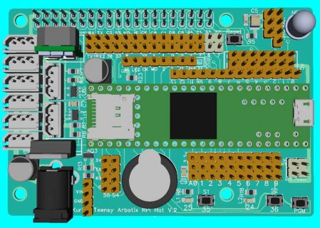
Also in addition, in Diptrace, there is the ability to do 3D previews of your design. For this I used Fusion 360 to create me a part to represent the T3.6(or 5). Which I have as a step file. Which you can see in the following rendition:
T3.6-RPI-Hat.jpg
 

Attachments

  • Teensy 3.6 v3.zip
    220.1 KB · Views: 390
In the meantime, you can also use my Eagle Library for the relevant parts, if you like.

Not sure if anyone would find it useful, I also have some part layouts for Diptrace. Although I also use some of the other Eagle ones where I then convert to diptrace...

Thanks for your replies. I actually found this breakout which was very useful as all I wanted to know was how the pins are spaced relative to eachother.
https://forum.pjrc.com/threads/38336-Preview-of-3-5-amp-3-6-Breakout-boards-Feedback-welcome!
 
Thanks Paul for putting the schematic together and releasing ... very useful.
Is the 32.768KHz crystal for RTC included on T3.5 and 3.6, or needs to be added by me ?

and thanks @Constantin - your eagle files will be very helpful too.
 
great thanks. I'm using the Sparkfun T3.1 adapter shield as a quick and dirty means to test / develop on my T3.5 and it wires in 3V coin cell holder. It actually comes with a loose 32.768kHz crystal, but I guess that's now relegated to my ever growing pile of spare parts ! :)
 
Last edited:
The man will have to reply, but when my beady eyes first glanced at the schematic, assumed that the other 2.2uF cap was providing stab.

My T3.5s seem to work just fine, and some recent regressions seem stable in environmental (or is that just mental?) chamber to -15C.
 
Good point. But, gonna guess that the ESR is more important than the cap value. Or empirical phase margin test data supports cap value. Or no issue because reg close to load. Or typo. Or space aliens.
 
...a minimum 1 uF bypass capacitor required at the input to the LP38691. The schematic shows a 0.1 uF capacitor employed. What's up with that?

There's actually a 0.1 uF and a 2.2 uF in parallel. Look a little lower on the schematic, near the TPD3S014 to find the other capacitor.

Even though they're shown relatively far apart on the schematic, each near only 1 chip, on the PCB layout these 4 parts are located close to each other. Both of these chips want capacitance at their inputs for stability. The 2 capacitors are effectively in parallel and provide a 2.3 uF input capacitance seen by both chips.
 
you may like to fix the minor typo on the schematic next time around:
pin 23/A9 OK
pin 22/A9 should be A8
 
There's actually a 0.1 uF and a 2.2 uF in parallel. Look a little lower on the schematic, near the TPD3S014 to find the other capacitor.

Even though they're shown relatively far apart on the schematic, each near only 1 chip, on the PCB layout these 4 parts are located close to each other. Both of these chips want capacitance at their inputs for stability. The 2 capacitors are effectively in parallel and provide a 2.3 uF input capacitance seen by both chips.

As has already been pointed out, I guess one would have to be very careful cutting the 5V input to the LDO for non-USB power. I am not sure how careful, because it is not clear where the trace to be cut is on the 3.5/3.6.
 
Of course you should always be careful when holding a sharp knife in your hand. But as for the safety of Teensy, those pads you cut apart are on the edge of the board. Make your cutting motion away from the rest of the circuit board (and of course your other hand) to avoid damage.
 
if you're talking about cutting the pads to isolate VUSB from VIN .... yesterday I had reason to do did it to my T3.5 . I can confirm it's a cinch with a typical razor knife, and due care.
 
I must confess, that I avoid razors that are too sharp to be left alone. So I disconnect the two Pads with an old broken (sharper) screw driver. Moving it forward-backward until the two pads are disconnected. The fact that, some solder-mask is removed does not bother me, it helps to bridge the disconnection is needed.
 
Status
Not open for further replies.
Back
Top