Validating a new breadboard break out board.

Status
Not open for further replies.

DaQue

Well-known member
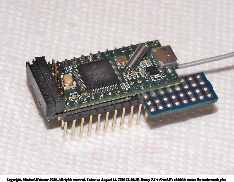
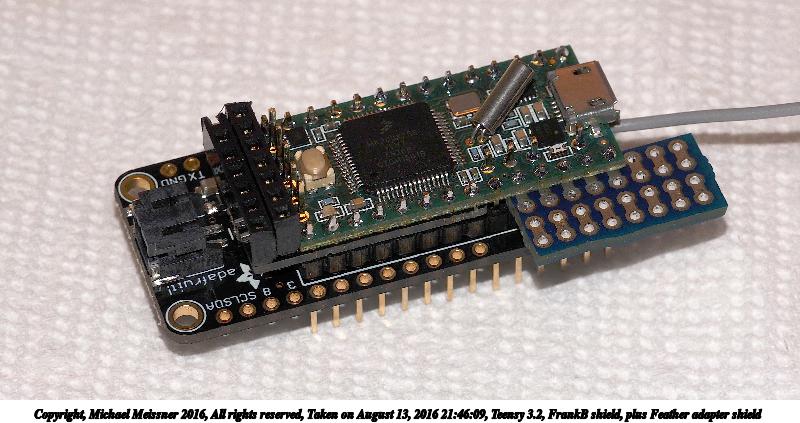
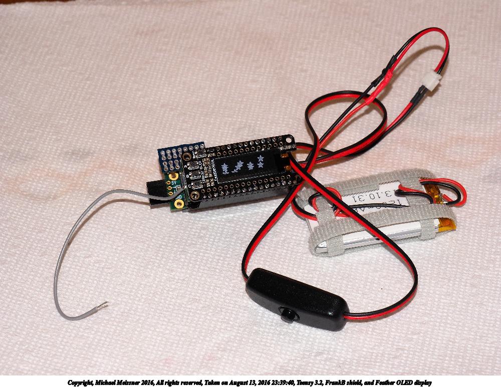
This weekend I think I will make a 3.5/3.6 version of this breakout (edit: not mine but the style I want to make, castlalted)

https://www.oshpark.com/shared_projects/Gnvbt7io


I want to fully validate it before I share it on Oshpark and looking for ideals on the best method to insure I caught any mistakes. Right now I am leaning to a led and resistor on every IO pin and just writing a sketch to light them one at a time and see if any other pins toggle(using pinmode Input). I think I will put a 100k in parallel with the led to make a decent pull up. One pin output mode at a time the rest input. Would that be a good enough test to release it? I will lay out a two skinny boards with the leds and resistors at the same time.


What would be a good way to test the rtc battery breakout besides just using an ohm meter?


USB lines won't be broken out.
 
Last edited:
Making the LED bars would beat pin to pin testing for continuity.

at first glance I assumed it was a 24 pin long unit setup to match a T_3.6 pinout - but see that isn't the case. That would be a total re-write but perhaps a worthy effort? Where new T_3.6 outer pins came from T_3.2 bottom - with the middle bar holding some others. Obviously not 1::1 mapping - but would have some use swapping a T_3.2 for a 3.6? My most used breakout board has a T_3.1 setup to allow use during the K66 beta - as far as it went.
 
I see a couple traces right next to the board output cut-outs. The reset signal also seems to touch the pads, and the ground fill looks like it comes extremely close to the pads. Maybe these are fine... but might be good to review the design rules you're using and run any DRC again, just in case.
 
I just want to make the bottom IO pads breadboard friendly as cheaply as possible. If there was a option to buy a physically larger Teensy's with all the pins breadboard friendly I would go that route. It it's two expensive (4 sq inches is my guess) there is an excellent kit breakout on Tindy too that I will just use. It's close to my ideal solution but I have a couple personal preferences I would do a bit different.
 
Thanks Paul, that's not my version. I will check when I make mine. It was just a link to show the kind of board I was going to make from scratch. If I do share it the Kicad library I found for Teensy's is MIT license I guess I need to credit him if I share on Oshpark.
 
breadboarding will all T3.x pads

Has anyone tried inverting the board on longer headers (to allow the electronics to clear the breadboard) and then using a double-row-SMT-header to connect to the pads on the now accessible 'bottom' of the board?
SMT_VR_DR_header.png
Then you could have a cable that transfers these to other columns on the breadboard without having to solder the Teensy to a breakout board (although the inverted layout on the main pins would take some getting used to).

Way beyond my pathetic soldering skills but I think the 2.54 mm pitch Tyco series would hit the pads OK even if they're not as wide as recommended.

http://www.farnell.com/datasheets/1498835.pdf
see page 110 (looks like stacking headers suitable for ensuring clearance for the main pins are on the next pages)
  • DR=double-row
  • VT= vertical
  • SMT= d'uh

A female socket block might be easier for end use but I'm not sure if the soldering would be too difficult.

Note: Sparkfun Header kit includes such a part: •1x 2x7 right-angle SMT header, for the surface mount pads on the back of the Teensy 3.2
 
Last edited:
@oddson one trick with trying to solder surface mounts like those headers by hand is a felt tip flux pen. Mark the pad and pin you want to solder and it makes it harder to bridge by accident since those two parts will wet before anything else if you have a shaky hands moment.

Proper answer of course is solder paste, but flux pens last longer in the tool drawer.

@Paul, given this comes up often is it worth adding a suitable SMT header set to the store? Though guess people will then start lifting the pads more often.
 
Has anyone tried inverting the board on longer headers (to allow the electronics to clear the breadboard) and then using a double-row-SMT-header to connect to the pads on the now accessible 'bottom' of the board?
View attachment 9939
Then you could have a cable that transfers these to other columns on the breadboard without having to solder the Teensy to a breakout board (although the inverted layout on the main pins would take some getting used to).

Way beyond my pathetic soldering skills but I think the 2.54 mm pitch Tyco series would hit the pads OK even if they're not as wide as recommended.

http://www.farnell.com/datasheets/1498835.pdf
see page 110 (looks like stacking headers suitable for ensuring clearance for the main pins are on the next pages)
  • DR=double-row
  • VT= vertical
  • SMT= d'uh

A female socket block might be easier for end use but I'm not sure if the soldering would be too difficult.


That's actually a pretty cleaver idea. The program button would be hard to get to but you seldom need it. Good idea!
 
Making the LED bars would beat pin to pin testing for continuity.

at first glance I assumed it was a 24 pin long unit setup to match a T_3.6 pinout - but see that isn't the case. That would be a total re-write but perhaps a worthy effort? Where new T_3.6 outer pins came from T_3.2 bottom - with the middle bar holding some others. Obviously not 1::1 mapping - but would have some use swapping a T_3.2 for a 3.6? My most used breakout board has a T_3.1 setup to allow use during the K66 beta - as far as it went.

IIRC, that board came out before the 3.5/3.6 were announced, and I believe the 3-4 boards that I've seen have the pins in a different order. It would be nice to have a new one that allowed the basic digital pins to be used the same. Obviously, you won't have Serial4, Serial5, SPI1, SPI2, etc.

Lets see:
  • Pin 25 is a PWM pin in 3.2 and not in 3.5/3.6;
  • Pin 26 is A15 in 3.2 and not an analog pin in 3.5/3.6;
  • Pin 27 is A16 in 3.2 and not an analog pin in 3.5/3.6;
  • Pin 28 is A17 in 3.2 and not an analog pin in 3.5/3.6;
  • Pin 29 is A18 in 3.2 and not an analog pin in 3.5/3.6;
  • Pin 30 is A19 in 3.2 and not an analog pin in 3.5/3.6;
  • Pin 31 is A20 in 3.2 and A12 in 3.5/3.6;
  • Pin 32 is a PWM pin in 3.2 and not in 3.5/3.6;
  • Pins 25, 32, and 33 are touch pins in 3.2 and not touch pins in 3.6 (and of course 3.5 doesn't support touchRead);
  • Pins 29/30 are SCL1/SDA1 in 3.2 while pins 37/38 are SCL1/SDA1 in 3.5/3.6;
  • Pins 26/31 are alternate pins for RX2/TX2 in 3.2 while there doesn't seem to be an alternative for the Serial2 pins in 3.5/3.6.
 
IIRC, that board came out before the 3.5/3.6 were announced

Indeed it did - I followed the link to picture before reading the 'not mine' part - but had the image give me the idea that seemed to fit with a castellated underside layout if the routing works.

Your list of the altered functionality points out valid issues preventing full drop in exchange - perhaps beyond digital numbers. And there is no second DAC1 on T_3.2. But everything T_3.2 would be there and go in the direction of the T_3.6 for reference.

One other note: When I used a T_3.1 to mirror the primary pins with the K66 Proto Beta I put female headers UP like the PROTO. This was a challenge to solder - I stuffed paste in the holes during assembly and luckily that did the job soldering under the BB. In any case with header that sandwich can only be soldered one side - would castellating the shared first 14 pins on the BB allow for better solder application with the male or female header plastic?
 
I can do solder through hole with just the soldering wire, but I'm not an expert. I've never used solder paste or attempted the soldering of SMT pins to the bottom pins. And my new electric de-soldering iron helps me undo mistakes and redo the soldering.

This classic post from Jimmayhaug in 2014 shows one method to bring the pins out:

While I haven't attempted soldering headers underneath the Teensy, I find the Teensy connector board #3 from FrankB is easy to solder due to its castlellated pin cutout. I cut some stacking headers or long pins down to two sets 16 pins and one set of 5 pins with my diagonal cutters. I use my rotary tool to smooth off the edges, and put the headers into the Teensy, and solder them underneath. I flip the Teensy over and melt solder over each of the castlellated pins to make a connection. Finally, I put some normal headers on the two rows of 5 pins.

Here is a slightly more complex job to attach the FrankB headers, the Prop Shield and the Adafruit Feather adapter.

First solder long pins to the standard 14/14/5 rows on the Teensy, solder the FrankB header underneath, solder a wire to the reset pin, and solder a small breakout board on the side. Unfortunately,, I did not think to take individual pictures of the steps:
2016-08-13-21-18-001-electronics.jpg


Here is an underneath view:
2016-08-13-21-19-002-electronics.jpg


Then attach the feather adapter:
2016-08-13-21-46-003-electronics.jpg


Finally attach headers for the Feather adapter and the prop shield underneath the Teensy with 90 degree headers for the sound and LED outputs:
2016-08-13-23-39-004-electronics.jpg


The combination of 4 boards plus spacing is a little tight, and the long pins that I have are just barely enough to mount into headers.
 
Last edited:
IIRC, that board came out before the 3.5/3.6 were announced, and I believe the 3-4 boards that I've seen have the pins in a different order. It would be nice to have a new one that allowed the basic digital pins to be used the same. Obviously, you won't have Serial4, Serial5, SPI1, SPI2, etc.

Lets see:
  • Pin 25 is a PWM pin in 3.2 and not in 3.5/3.6;
  • Pin 26 is A15 in 3.2 and not an analog pin in 3.5/3.6;
  • Pin 27 is A16 in 3.2 and not an analog pin in 3.5/3.6;
  • Pin 28 is A17 in 3.2 and not an analog pin in 3.5/3.6;
  • Pin 29 is A18 in 3.2 and not an analog pin in 3.5/3.6;
  • Pin 30 is A19 in 3.2 and not an analog pin in 3.5/3.6;
  • Pin 31 is A20 in 3.2 and A12 in 3.5/3.6;
  • Pin 32 is a PWM pin in 3.2 and not in 3.5/3.6;
  • Pins 25, 32, and 33 are touch pins in 3.2 and not touch pins in 3.6 (and of course 3.5 doesn't support touchRead);
  • Pins 29/30 are SCL1/SDA1 in 3.2 while pins 37/38 are SCL1/SDA1 in 3.5/3.6;
  • Pins 26/31 are alternate pins for RX2/TX2 in 3.2 while there doesn't seem to be an alternative for the Serial2 pins in 3.5/3.6.

It's planned to be a 3.5/3.6 board that it's soldered under and this style of board means all IO pins 0-39 will share the same x y pin location. They will really just be a hole for a pin that's not routed anywhere.

There is a very good chance I will have to just pass on this if I have to resort to 4 layers to get it done which seems likely. I don't think I can fit 28 lines through the narrow part where the cut outs are and the 5 holes across the middle. That is running all of them out the end opposite the USB connector so you can still plug it in with another board flush to the bottom of the Teensy. There is already a good breakout on Tindie for $15 https://www.tindie.com/products/loglow/teensy-3536-breakout-revision-a-standard/?pt=full_prod_search for $15 each and Oshpark for a 4 sq inch 3 pack of 4 layer boards would be $40 or $13.33 each. Not the drastic savings I was hoping for. SeeedStudio i an option but I would have to get 40 of them up front and pay about $4.10 each. I'll never use 40 of them. Seeed pricing is based on fitting 4 in a 10cm sq quote from their order page for 4 layer with Half-cut / Castellated Holes. I think I will just call the idea busted and move on. That's a shame I just ordered 200 0805 leds... The best idea so far I think is oddson's , just put tall headers out the top and plug it in upside down and use smt dual row headers on the pads.
 
Status
Not open for further replies.
Back
Top