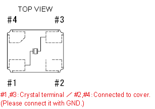
Hi everyone,
I'm currently designing a Teensy on a board, and have a question regarding the PCB design for the crystal. From that I have read:
1. Ground plane under crystal
2. No digital signals below crystal
3. No parallel lines with crystal signals
I am not certain if I should be grounding the Inner plane (purple) with the bottom ground plane (red).
Is this design sufficient?