SPI and I2C distorted signals Teensy 3.5

Status
Not open for further replies.

Eheran

Member
I have some issues with both SPI and I2C.
First 3 pictures are I2C, the next 4 are SPI (MISO, MOSI, 2x clock).
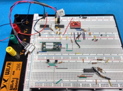
Hardware: Teensy 3.5 with: SSD1306_128X64 OLED, DS3231 RTC, BME280 sensor and on SPI is a nRF24L01+ transceiver.

Look at those artefacts in I2C and its slow rise time... what is going on there?
The SPI doesnt look too good as well, but I dont know if that might be normal.
I2C has 4,7k pullups (see picture) and it doesnt seem to be the external hardware causing this, it works fine with atmega328p (Pro Mini) and still persists with a different radio and BME280.
Both I2C and SPI cause intermittent issues due to this, so RF not receiving and the sensor not reading data once in a while.
Im up to suggestions now after trying to find the problem for lots of hours and reading nearly everything about issues with nRF24L01+.
So... wiring or the teensy 3.5?
I could pull the Teensy 3.5 out and "hotwire" a Teensy 3.2 in the same slot as well as redo the wires...
But for now I want to see what you guys say. And others can find this thread if they happen to get such weird problems as there is nothing like this so far.


I2C SCK.pngI2C SDA.pngI2C SDA2.png
SPI-MISO.pngSPI-MOSI.png
SPI-SCK.pngSPI-SCK2.png
WP_20171012_21_46_33_Raw.jpgWP_20171012_21_46_41_Raw.jpg
 
While the waveforms are obviously less than perfect, they are not *that* bad, and unless you have something that requires a very precise timing on the rising edge, I don't see why a little bit of distortion would cause issues.

Can you display more than one signal on your scope to see if there is some issue elsewhere? With SPI, the relationship of various edges on the CLK, MOSI/MISO and CS/SS line can be important.
 
you should be using 2.2k pullups for teensy, atmega is 5v so 4.7 is ok for that, teensy is 3.3v so it can affect the bus

i doubt there is spi issues with t3.5, teensy is very fast, try to put a delayMicroseconds(10); between every SPI.transfer() and see how that works, the SPI and cpu are very fast so you need to slow down the speed and/or give the chip time to process the commands

are you using SPI Transactions?

FWIW, I've tried to drive two OLED 128x128 display (using the uncanny eyes program that displays two moving/blinking eyes), and some of the displays, I had to slow the processor clock down to 24Khz to get it to not corrupt the display. I finally gave up on the OLED displays, and went to TFT that have worked at all speeds, including the 3.6 over-clocked to the fastest speed. You might try playing with the processor speed, putting in delays, and/or use a slower SPI bus speed (look at SPI.beginTransaction).
 
ive had no issues with master/slave spi setup overclocked to 168/240mhz using spisettings of 75,000,000, although id really like to know the real speeds later on lol
 
Few things come to mind.
1. Your scope can play tricks on you if your not careful how your measuring.
2. I have heard mention several times of power modes with the SPI. You could be in low power mode.
3. I see you wired the LCD to 3.3V, is it a 3.3V LCD? If the inputs are set up for 5V with resistors you may not be driving it hard enough with 3.3V.
 
Those waveforms look pretty normal to me. Rise times on I2C are expected, because the signal rises only due to the pullup resistors. I see what looks like a 1/10 of division and the top says 2.00us. A 0.2 us rise time on I2C is pretty decent.

The SPI signals also look ok. From the scale, it looks like 12 MHz rate. Yeah, there are some little artifacts like this:

SPI-SCK2.png

That sort of minor weirdness is almost certainly due to the wiring construction, especially where the signals aren't accompanied closely by a ground wire (or ground plane on the next PCB layer). It's also important to remember the scope probe, and especially the lengthy ground clip wire, can also contribute to these minor effects.

My guess is there's probably a much sharper spike at the beginning of that little weird area, which you can't see due to this scope's limited bandwidth (plus the probe's bandwidth), and perhaps also limited by imperfect probe compensation. A 500 MHz Keysight scope with properly compensated 700 MHz probes would likely show a different, even worse picture. Then again, with higher bandwidth you really can't use a ground clip on the scope probe. High bandwidth probes expose a ground shield right near the probe tip, and the make such measurements you really need to arrange for the board's ground to touch right near the probe's shield.

Looks like you're also getting some cross talk.

I2C SDA.png

This sort of issue is also very common with point-to-point wiring (large area between signals and their grounds) of signals without any termination resistors. A higher bandwidth measurement would probably show these are even worse. But still, it they're not getting near the logic threshold, probably not an issue. I2C also is almost always implemented with low-pass filters inside the chips, to reject these sorts of very short transients which are common on I2C signals.

The one thing I see here that really is bizarre is this info from your scope:

I2C SDA.png

This is shown on a screen where the waveform has 4 rising edges on a display that's 2 us/div. Maybe that's a frequency counter looking at edges spanning a *MUCH* wider time scale than the scope. That's the only explanation I can imagine for showing a frequency with a period that's FAR long time than the entire horizontal range the scope is showing at least 4 cycles.

Anyway, these signals look pretty normal for this type of construction and casual/easy probing technique. I2C always involves rise times. If you want beautifully square SPI signals, you really need to do a lot more work to run ground return paths closely with every signal (like a 4 layer PCB with the inner layers dedicated to power & ground planes), and eliminate the ground inductance on your probe, and even then you'll see ringing and other high speed issues that are only really resolved by a lot of careful work to add transmission line impedance matching resistors.
 
So... its not the signal integrity, wiring, teensy, ...
Its some fancy-magic-RF-voodoo and the I2C issue was just an add-on to confuse even more.
Example:
RF and TX running and just sending at max rate to see data loss... Scenario: Intermittent issue, maybe 50% packet loss. I touch the insulated TX data wires or antenna: 0% packet loss. I touch something else on the TX unit: Might do nothing or 100% packet loss or 0% packet loss. If I move very slow and careful I can get between 50% and 0% packet loss by getting close to the TX wires (no touch). Works for Vcc, GND, Data and CS/CE wires.
Different transceiver (totally different model, no PA/LNA): I get close to the TX PCB of the transceiver and get rising packet loss from 0 to 100%....
Doesnt matter if they share the same ground or one is floating, tho floating makes it less sensitive.
I move it around... suddenly: Problem gone... works solid, 0% packet loss while touching/poking/leaving alone. How to get intermittent-mode back? Uh... just happens suddenly, random? Maybe some special move, orientation? Bending/twisting the PCB a little and pressing on every part to check for bad connections doesnt do anything in both intermittent and working "mode". Both "modes" survive power cycles. Units with 100µF cap on GND<->Vcc work a lot better. Going up to 500µF does not improve it further.

Any ideas how to get this capacitive coupling(?) to stop? And why it is so weird intermittent?
 
you shouldnt only rely on the ground from the power rail as common, in some events running a ground FROM teensy to the external CHIP may fix those issues
 
I have a ground from teensy/Atmega/Coretex M0 directly to the unit.
Should I:
Use a different GND pin? Somehow solder a new wire to the tiny QFN20 4x4 package and run it to the unit? Use analog GND? GND directly from the floating power source (battery)?
 
So... its not the signal integrity, wiring, teensy, ...
Its some fancy-magic-RF-voodoo and the I2C issue was just an add-on to confuse even more.
RF stuff can be tricky and like a black magic sometime. If you are not limited by bandwidth, you can cut your SPI clock frequency in half, or less, and see if that makes any difference. My guess is no, but you can never be certain until you try it.

Another wild guess is that you probably have a grounding/shielding issue somewhere, based on some of your symptom descriptions.

For shits and giggles, here is the remnant of some prototyping (some stuff has been removed already days ago) and SPI was running just fine at 5 MHz.

Waveforms of this circuit were posted in: https://forum.pjrc.com/threads/46746-short-pulses-on-the-MOSI-line-after-every-8-bits
 

Attachments

  • circuit.jpg
    circuit.jpg
    97.4 KB · Views: 95
Update:
The touch issue was mostly due to missing pinmode output for CE and CS in those testmodes... mostly... thus irritating because if you touch the SMD-parts you can get it to stop too...
But this was not the initial issue of intermittent fault, they always were set to output in the programm. But it seems like the AutoAck feature caused issues. It has been running fine now for several hours, 1000's of transmissions without a loss with both PCB-antenna-units and those with PA+LNA + real Antenna. I will see if this is working consistently now and update if not.
 
Nah, it didnt help at all, nothing changed. Randomly not receiving. I have 2 receivers here (Teensy + Pro Mini Atmega328p), they both independently miss signals as well as the transmitter droping some. Today the Teensy RX stoped working for solid 3h... after which it was fine again...
 
Status
Not open for further replies.
Back
Top