Teensy 3.2 SPI pins

Status
Not open for further replies.

summers

Active member
Do the teensy 3.2 SPI pins need to be used in groups?

E.g. there are two SPI channels in hardware that look like (SCLK,MOSI,MISO) (PTD1,PTD2,PTD3) and (PTC5,PTC6,PTC7).

So numbers suggests they come in sets of 3, and the greying out on the teensy pinout card, also suggests sets. But the data sheet describes both as SPI0.

Question is can I use (PTD1,PTC6,PTC7), this avoids PTC5 which is wired to the LED?

Reason I ask is I'm getting nothing sensible from the chip right now - and not sure if its a bad connection ....

[And I presume I can use which ever SSEL I want with either, as thats low bandwidth ...]
 
Last edited:
There is only one SPI instance available in the Teensy 3.2. It is by default mapped to PTC5 (pin13), PTC6(pin11), and PTC7(pin12). But you might remap some or all signals to alternate pins via the signal multiplexing unit. Thus, the SPI clock might be rerouted to PTD1 which is pin 14 without affecting the other pins. Most SPI libraries allow to define the pins which you want finally to use.

Everything is well documented on this page. (RTFM!!!)
 
Hi,

Thanks for the link - I havn't come across that.

I must admit I'm developing on mbed, so I read the manual: https://os.mbed.com/docs/v5.7/reference/spi.html

And browsed through to the source code: https://github.com/ARMmbed/mbed-os/...ARGET_K20XX/TARGET_TEENSY3_1/PeripheralPins.c

That defined the pins I refered to. I checked the schematic: https://www.pjrc.com/teensy/schematic.html and so where the pins point.

Read the data sheet: https://www.nxp.com/docs/en/data-sheet/K20P64M72SF1.pdf with the pinout (chapter 8).

Even read the Reference manual: https://www.nxp.com/docs/en/reference-manual/K20P64M72SF1RM.pdf not the full 1377 pages you understand, just chapter 45 on SPI.

But turning to the F*ing Manual, as you so politely put it [I note you are french, but please realise this is quite insulting in english, just as if I went on about "merde" in french - so only use acronyms like this if you know what they mean and wish to cause offence].

But Pauls manual, the first table says (SCK,MOSI,MISI) = (13,11,12) or the alternate (14,7,8). Now using the schematic linked above these can be mapped to the cpu pin out (PTC5,PCT6,PTC7) or alternative (PTD1,PTD2,PTD3) - which is what I posted in my first post ..... [hmm maybe I can read afterall, what a thing education is].

So everything written says the same (all be it the mbed source code orders differently). The important bit is that the arm cpu has hardware SPI, and using hardware SPI is far better than bit banging the protocol. Now your post does contain one useful bit of info, that the CPU only has one SPI, which is what the Data Sheet hints at (all called SPI0).

Now little is said about how to use the alternate SPI pins, we learn from the data sheet that we need to put the pins into Alt2 mode - but thats all. Now PJRC hasn't said much on pin mode I can see. Mbed says nothing I can find on pin mode. But both these sets of people know this.

No one has said anything about if I can mix between the alternate pin outs for SPI0.

So what have we learnt here, well we can all read - lets agree on that.

What I was asking for was if anyone had practical experience.

Hey I can debug the hardware myself if needed, loop back on MOSI<-->MISO, scope on SCK, Scope on MOSI with SCK trigger, etc - but these are a hassle. Instead shall we try and help each other rather than barbed insults?
 
I didn't mean to offense whomever. As I had understood it, "RTFM" was a sloppy, friendly, and rather ironic hint. Obviously, it is not always, so I'll have to take care.

In your initial posting, you didn't write that you were using mbed, thus, by extrapolation from 95% of users in these forums, I thought that you were developing using the Teensyduino plugin and the Arduino IDE, where all pin definitions (default and alternate) are included in the Teensyduino core files and the included libraries, and the use of all that is well documented on the PJRC website.

By writing
Thus, the SPI clock might be rerouted to PTD1 which is pin 14 without affecting the other pins.
I thought I had stated clearly that you can in fact mix the pin sets, please accept my apologies if I haven't been clear on that. The K20 has an internal signal multiplexer which allows to connect different signals from the internal HW blocks to the pins. That means that you decide by setting up the port control module, which of the up to eight alternate connections of one pin to internal hardware will be activated. From the table on p207 in the reference manual, you see that you might route the internal SPI clock signal either to PTC5 by choosing ALT2 for that pin or to PTD1, also by choosing ALT2. Independent from that, you might with the same procedure set MOSI to either PTC6 or PTD2 and MISO to PTC7 or PTD3. The manual states also clearly that, although technically possible with the corresponding port control settings, you never should route the same signal to more than one pin at the same time.

So, you can imagine the pins of the Teensy and the internal hardware not at all connected by default. Connections are made through the port control module which acts as a kind of cross-bar switch which allows to "route" almost every individual internal signal to several pins, depending on your choice and needs. Again, pages 207-209 of the reference manual are your friends.
 
OK I've now wired the CLK out by PTC5 = 13 the LED. I've also checked what I get back *whilst* I write instructions.

So I take the CS line low. Then write the 8 bit command: 0x1e, which means reset. What I get back during this is 0xfe - that e is a surprise, it means that I am getting data back.

I pause for 3ms as per the spec after a reset. Then whatever I send, I only get 0xff back.

Whats odd, is after I've finished - maybe I take the CS high to deselect the chip again. But whats odd is that the LED, the clock is on, e.g. hi. Now I'm in SPI mode 0, I though the default clock was low? So at start of clock goto 1, 50% through cycle go to zero, and its the rising edge that defines the edge. Now with such a clock, shouldn't I always end up low, e.g. on zero?

Oh yes in the github teensy definition above, that defines the SPI pins. I think the 3rd column is the pin mode - so for SPI it is selecting mode Alt 2, which is correct. I need to dig through the headers though to see if that is how the data is defined ....


Ah - fig 5 of http://www.hobbytronics.co.uk/datasheets/sensors/MS5611-01BA03.pdf does indeed say I should get 0xfe back on a reset - the DO drops when the DI drops at the end of 0x1e sent ...

Changing the code to just send the reset (0x1e) then stop - and the clock end up low. So clock seems correct there. In the full sequence I'm sending:

0x1e - Reset
Pause 3ms
0xa00000 - read prom 0 - and 0x0000 is the 16 bit read out
0xa20000 - read prom 1
0xa40000 - read prom 2
0xa60000 - read prom 3
0xa80000 - read prom 4
0xaa0000 - read prom 5
0xac0000 - read prom 6
0xae0000 - read prom 7 - its only after this write that the clock gets left high
 
Last edited:
Hi Paul,

Yes - all mbed code. But yes - having seen where the SPI clock ends on mbed, and I can see that there is something very wrong in the mbed code.

I had a quick look at arduino the other day, but my brain hurt - or rather its set up in a bit of a fluffy way for my liking. Anyway I think I'll dig into it in more detail - whilst moaning at the mbed people. Pity in some ways, when I first used mbed, back in 2013 or so it was very good. Don't know if things have changed ...
 
For the Arduino - download the zip and extract to a clean folder - I do it on root of a second drive. Then install TeensyDuino to that folder and start Arduino? Fluffy?
 
Sigh. Last night was reading an application note about the pressure sensor, and the code to access it:

http://www.amsys-sensor.eu/sheets/amsys.fr.an520_e.pdf

It had the cryptic line:
csb_hi(); // pull CSB high to finish the command
Which I havn't seen documented.

Anyway tried that, and yes if I pull the chip select to high after *every* command I do get data back.

So the mbed SPI lib is reading correcly, just leaves the clock in an odd state.

and the MS5611 pressure sensor SPI interface seems a tad none standard. Its not a well known sensor (there is almost no documentation on it, and its not easy to buy), but works down to 10mb and has a 24bit sigma delta convertor.

Interestingly whenever the MS5611 is sent a command, it sends back at the same time 0xfe! I suspect because bit 8 of the command is called "stop" so the device has the command by bit 7, and so is sending its own stop back again! Wish this had been documented ...

Oh yes, on arduino, the bright colours, and large downloads, aren't my thing .... have to admit I'm more a man who reads documentation, and then just implements the code - so I prefer 90% reading first. This CS going high to complete a command is a good example - can't see how one would find it without reading it ...

Anyway I've started the arduino download - I'll produce the same code in android then compare ...
 
Ah, the data sheet says:
The CSB pin can be pulled high after the command is sent or after the end of the command execution (for example end of conversion).
So what does that mean to you? Anyway at least solved now.

Now to check the CRC4 check ... (0x13)
 
Thanks for the link, its helpful to read some elses code. His isn't well commented, e.g. the importance of
Wire.endTransmission();
. When reading the PROM, he doesn't do the checksum. Also there is some integer arithmetic that can be simplified (e.g. int*256/128), by reordering you avoid overflow problems.

I'll post mine when finished, hopefully end of today, been fixing the car this morning ...

Oh yes, should have said, I'm doing SPI rather than I2C, as I2C needs two pull up resistors. Mine has to be minimal volume, to fit in the kinder egg. And it seems easier, to have the two extra SPI wires over the 2 resistors in I2C.
 
Check the second link out - that's has a spi implementation. Just wanted to give you some samples.
 
Ah yes - I missed the second one, that is far cleaner code. Close to mine.

I've just got raw D1 and D2, which is what I need for flight. But I'll add the conversion to physical to check.

This MS5611 really is a bit finicky, but is easy to diagnose, if it ever just puts out 0xff all the time - then its gone into error.
 
Many people, including me, use Arduino's "external editor" feature in File > Prefs. It disables Arduino's rather primitive editor and causes it to monitor the files for changes, so you can use an editor of your choice.

Yeah, lots of Arduino stuff revolves about libraries that have more code than you'd probably write from the ground up. But many of these extra features like SPI transactions solve some very thorny problems that you might not anticipate. It's a large ecosystem of code, with quite a lot of work put into making things work nicely together with minimal user effort.
 
OK, check out my cryptic code here:

https://os.mbed.com/users/summers/code/MS5611/

Note it hasn't been checked, mainly because the output I get right now is:

Hello World!
Prom(0): 2104
Prom(1): 46715
Prom(2): 49015
Prom(3): 28275
Prom(4): 26203
Prom(5): 32942
Prom(6): 27030
Prom(7): 11163
D1 = 16680571
D2 = 16678966
Temperature = 285.698853 deg C
Pressure = 13.344305 mbar
The problem is that both D1 and D2 are close to full range (2^24) and this means I'm getting silly numbers - but its the raw D1 and D2 integers that are driving it ....

Oh yes, note that the CRC4 sum is *very* odd, it only includes something like the first 4 bits of the PROM[7]. To my mine thats a coding error, but its applying what is in AN520 - and it passes the test. Assuming all chips have this error, I can see why many libraries skip the CRC check.
 
OK, found the problem. Its that to read the ADC values you need to send 4 zero bytes! The first is the command to read, to which the MS5611 responds 0xfe, the next 3 bytes are to clock out the 24bit result.

My mistake was to only send 3 zero bytes, and take the 0xfe as part of the data.

Think what I learn from this is there are two replies that the MS5611 gives that you need to take care with 0xff means error, the sensor isn't happy. and 0xfe which means command received. So if you *ever* see either of these two bytes, take care and watch closely.

My code is : https://os.mbed.com/users/summers/code/MS5611/

Example output:

D1 = 8845258
D2 = 8483882
Temperature = 21.634636 deg C
Pressure = 994.063626 mbar
D1 = 8845448
D2 = 8483382
Temperature = 21.618525 deg C
Pressure = 994.066257 mbar
D1 = 8845226
D2 = 8483798
Temperature = 21.631929 deg C
Pressure = 994.049779 mbar
D1 = 8845388
D2 = 8483496
Temperature = 21.622198 deg C
Pressure = 994.061929 mbar
D1 = 8845440
D2 = 8483484
Temperature = 21.621811 deg C
Pressure = 994.072598 mbar
So there is noise on there of a ~20ubar, which is pretty good ...

Now to move onto the SD card, and decide wether to use arms Little File System ....
 
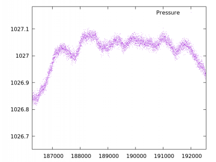
Havn't had time to do any more code, but as pressure is working here is a ploty of pressure taken from today, the bottom axis is in seconds, and I take one measurement a second. You can see that its accurate to about 0.2mbar. With averaging looks like I'd get a smaller error.
presure.png
 
Am about to start programming the SD card. Now i was half thinking of doing this via the second set of SPI pins, so the pressure sensor is on one set, and the SD card on the other set.

Now won't access the pressure sensor and SD card at the same time, usually read the pressure sensor, and then write the results to the SD card.

Now the K20- guidance is that you can't use both sets of SPI pins at the same time. So I guess the question is can the signal multiplexer cope with switching from one to the other fairly quickly? I'm expecting both sets of pins will be in mode 2.

Now of course I could use the same set of pins, with just different CS pins - but I'd need to take more care with my wiring then. E.g. at the moment I've just got loose wire wrapped round each hole, at least until I decide what pins to use. For shared wires, probably want to mount proper headers, and crimp the different wires together ...
 
Well if you consider the alternate pins as an additional SPI bus it is possible, just dynamically setMISO/setMOSI/setSCK back and forth to have 2 busses :)
 
Status
Not open for further replies.
Back
Top