Hello everyone, this is my first post in the forums, since I only recently jumped onto the Teensy wagon 
I am currently designing a shield for the Teensy 3.6. This shield is for a robotics project and it will do a bunch of things but I mostly want to focus on 2 of those things which I could use some advice with:
1) Using Analog GND: One of the tasks I want to perform is to take a lot of REALLY fast readings of photodiodes. There is a separate board housing a bunch of LEDs and Photodiodes, along with two 32ch MUXes (ADG732) to handle them. The interface between this separate board and my shield is a FFC cable with 14 positions (10 control lines the muxes, 5V, GND, LED input signal and PDs output amplified signal). The child board housing the LED/PDs also provides each PD with a trans-impedance amplifier in the following config:
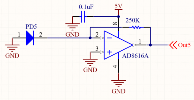
My firmware will cycle through all the PDs as fast as possible, and take readings from each one. In my original design I had tied AGND with GND in my shield, but then realized this is not a good idea, since they are already related within the T3.6 board. Getting the least amount of noise on the signal that I get from the PDs amplification circuit is important. With this in mind, should I actually be using the AGND in the FFC cable instead of my normal GND ??
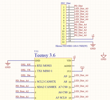
In this pic, I would replace the normal GND on position 14 of the connector with a "signal GND" which would be connected to the AGND pin. Would this improve the SNR on the photodiodes signal ??? The normal GND in the shield serves some other low power circuitry and a 10V regulator that gets 12V as input.
2) How to protect input pins: Another task happening in my shield is the amplification of some Wheatstone bridges. This is carried out by the following circuit:
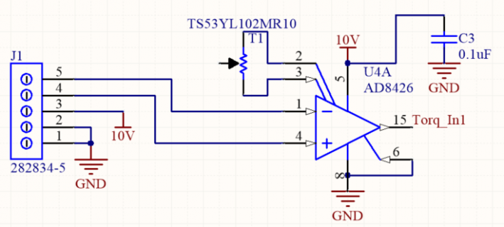
I initially had this instrumentation amplifier powered with 3V3 so that I'd guarantee that no matter what the gain is set to (by the external trimmer pot) I would never output anything greater than 3V3, since Torq_In1 then is connected to the analog pins. When the bridge is balanced, the input pins are around 5V, hence I can't power the AD8426 with 3V3. I've decided to just power it with the 10V line, but now if the gain of the amplifier is set too high, you could kill an analog input by getting more than 3.3V in the Torq_In1 signal.
What is a good way of protecting the analog pins if my signal could potentially go up to 10V??? I'd like to make this fool proof so if someone touches the Gain trimmer pot I won't end up with a dead Teensy.
BTW, I suppose I could also use the AGND for this amplification circuit to reduce the noise here as well ?
Let me know if something is unclear or if I should provide more details regarding my design.
Thanks in advance for your time!
Pedro
I am currently designing a shield for the Teensy 3.6. This shield is for a robotics project and it will do a bunch of things but I mostly want to focus on 2 of those things which I could use some advice with:
1) Using Analog GND: One of the tasks I want to perform is to take a lot of REALLY fast readings of photodiodes. There is a separate board housing a bunch of LEDs and Photodiodes, along with two 32ch MUXes (ADG732) to handle them. The interface between this separate board and my shield is a FFC cable with 14 positions (10 control lines the muxes, 5V, GND, LED input signal and PDs output amplified signal). The child board housing the LED/PDs also provides each PD with a trans-impedance amplifier in the following config:

My firmware will cycle through all the PDs as fast as possible, and take readings from each one. In my original design I had tied AGND with GND in my shield, but then realized this is not a good idea, since they are already related within the T3.6 board. Getting the least amount of noise on the signal that I get from the PDs amplification circuit is important. With this in mind, should I actually be using the AGND in the FFC cable instead of my normal GND ??

In this pic, I would replace the normal GND on position 14 of the connector with a "signal GND" which would be connected to the AGND pin. Would this improve the SNR on the photodiodes signal ??? The normal GND in the shield serves some other low power circuitry and a 10V regulator that gets 12V as input.
2) How to protect input pins: Another task happening in my shield is the amplification of some Wheatstone bridges. This is carried out by the following circuit:

I initially had this instrumentation amplifier powered with 3V3 so that I'd guarantee that no matter what the gain is set to (by the external trimmer pot) I would never output anything greater than 3V3, since Torq_In1 then is connected to the analog pins. When the bridge is balanced, the input pins are around 5V, hence I can't power the AD8426 with 3V3. I've decided to just power it with the 10V line, but now if the gain of the amplifier is set too high, you could kill an analog input by getting more than 3.3V in the Torq_In1 signal.
What is a good way of protecting the analog pins if my signal could potentially go up to 10V??? I'd like to make this fool proof so if someone touches the Gain trimmer pot I won't end up with a dead Teensy.
BTW, I suppose I could also use the AGND for this amplification circuit to reduce the noise here as well ?
Let me know if something is unclear or if I should provide more details regarding my design.
Thanks in advance for your time!
Pedro


