Need Faster Interrupt Handling!! >>>

Status
Not open for further replies.

AshPowers

Well-known member
I have an EPROM Emulation project that uses a 45ns NVSRAM module which is being used by another host computer for it's operating program. I am handling the NVSRAM contents via the Teensy 3.5.

I have 7 PI5A100WEX SPDT analog switches, rated at ~7ns switching period - NVSRAM is on the COMmon terminals. Two of these handle the 8 data bits, 4 are used for the 15 address pins, and the last one handles CE, OE, and WE.

On my scope I've been able to refine the coding/timing to get a single byte write to the NVSRAM within a 45ns window. This is the fastest I can get it to run before there isn't enough time for the address/data pins to settle and enough time for the WE to go low for full byte programming.

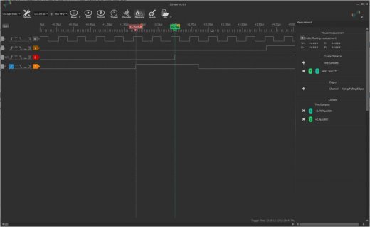
Timing01.jpg

The host processor is an HD6303YCP 8-bit microcontroller running at 3MHZ.

In the scope screen shot you can see each of the clock signals. The top is the 6303 clock, the second is the CE line (from the 6303 to the NVSRAM), the third is the write pulse from the T3.5 and the 4th is the signal that throws the analog switches.

The 6303 controls the NVSRAM output by using the CE line (OE cycles with the system clock - this is read-only for the 6303). The 6303 is accessing the NVSRAM when this line is pulled low.

There is about 340ns of time (between the green cursors, second row) where the 6303 isn't accessing the NVSRAM. This is on the lower end of typical - this ranges up to around 500ns but inconsistent.

The idea here is to use an interrupt to wait until the CE line goes high and then be able to sneak in a read or write in that time when the 6303 isn't accessing the NVSRAM.

I came across another page here showing how one guy was able to get the interrupts on this board down into the 132ns range.
https://forum.pjrc.com/threads/45413-ISR-latency-Teensy-3-1-and-3-6

But the code there is unintelligible for myself at a *rookie* level here and everything else I have been finding refers to the attachinterrupt function which is HORRIFICALLY slow and pinging in at around 550ns latency. Obviously this T3.5 can do MUCH better than that and I am going to need that capability to finish this project. 130ns interrupt latency + 45ns for the write/read cycle and I'm still under 200ns which in no case have I ever seen this 6303 access the NVSRAM between cycles any faster than about 300ns. Ironically, the read/write is so short that the 6303 doesn't fault but occasionally it drops communication through its SCI port during a read/write sequence. Fortunately there is no bus contention because of the switches but the 6303 does "hiccup" if you strip it's access to the NVSRAM in the middle of a read, LOL..

I have attached the source here: It is a very simple program that mostly does nothing other than just sit there so this ONE interrupt will be the only one I'll need to use. Address/Data read/write requests are handled through the USB/serial port via a serial.available code block in the loop().

Thank you so much in advance for your time and assistance with this!! This is the last step in completing this project and I'm very excited to put this to full use! :)

Code:
#define Data0 2
#define Data7 9
#define ADR0 31
#define ADR7 38
#define ADR8 14
#define ADR14 20
#define OE 22
#define CS 21
#define WRITE_EN 23
#define SWITCH 10


unsigned int integerValue=0;
char incomingByte;
int progaddress = 0;

void setAddress(int address) {
  uint8_t xlow = address & 0xff;
  uint8_t xhigh = (address >>8);
  for (int pin = ADR0; pin <= ADR7; pin += 1) { //sets output pins with data bits
    digitalWriteFast(pin, xlow & 1);
    xlow = xlow >> 1;
  }
  for (int pin = ADR8; pin <= ADR14; pin += 1) { //sets output pins with data bits
    digitalWriteFast(pin, xhigh & 1);
    xhigh = xhigh >> 1;
  }
}

byte readEPROM(int address) {
  for (int pin = Data0; pin <= Data7; pin += 1) { //set ardino data pins to read
    pinMode(pin, INPUT);
  }
  setAddress(address); // call to sub to set the address bits
  byte data = 0;
  digitalWriteFast(SWITCH, HIGH);
  digitalWriteFast(CS, LOW); //Turns the SRAM ON
  digitalWriteFast(OE, LOW); // SRAM OE ON
  for (int pin = Data7; pin >= Data0; pin -= 1) { // reads data on SRAM outputs into Arduino
    data = (data << 1) + digitalReadFast(pin);
  }
  digitalWriteFast(OE, HIGH); //disables SRAM data outputs
  digitalWriteFast(CS, HIGH); //Turns off the SRAM
  digitalWriteFast(SWITCH, LOW);
  return data;
}

void writeEPROM(int address, byte data) {
  digitalWrite(CS, LOW); //Turns SRAM ON
  digitalWrite(OE, HIGH); //Output Enable OFF
  setAddress(address); 
  for (int pin = Data0; pin <= Data7; pin += 1) { //sets data pins on arduino to OUTPUT mode
    pinMode(pin, OUTPUT);
  }  
  for (int pin = Data0; pin <= Data7; pin += 1) { //sets output pins with data bits
    digitalWrite(pin, data & 1);
    data = data >> 1;
  }
  digitalWriteFast(SWITCH, HIGH);
  digitalWriteFast(WRITE_EN, LOW); //pulls the SRAM W line low for a moment to program the data
  digitalWriteFast(WRITE_EN, LOW); //pulls the SRAM W line low for a moment to program the data
  digitalWriteFast(WRITE_EN, LOW); //pulls the SRAM W line low for a moment to program the data
  digitalWriteFast(WRITE_EN, HIGH);
  digitalWriteFast(SWITCH, LOW);
  digitalWriteFast(CS, HIGH);
  for (int pin = Data0; pin <= Data7; pin += 1) { //sets data pins on arduino to INPUT mode
    pinMode(pin, INPUT);
  }  
}

void setup() {
  Serial.begin(9600);
  
  pinMode(CS, OUTPUT);
  digitalWrite(CS, HIGH);
  
  pinMode(OE, OUTPUT);
  digitalWrite(OE, HIGH); //SRAM output enable pin.  HIGH = disabled
  
  pinMode(WRITE_EN, OUTPUT);
  digitalWrite(WRITE_EN, HIGH); // SRAM WRITE PIN
  
  pinMode(SWITCH, OUTPUT);
  digitalWrite(SWITCH, LOW);

  for (int pin = Data0; pin <= Data7; pin += 1) { //set ardino data pins to read
    pinMode(pin, INPUT);
  }
  for (int pin = ADR0; pin <= ADR7; pin += 1) { //sets address pins on arduino to OUTPUT mode
      pinMode(pin, OUTPUT);
  } 
  for (int pin = ADR8; pin <= ADR14; pin += 1) { //sets address pins on arduino to OUTPUT mode
      pinMode(pin, OUTPUT);
  }
}


void loop() {
 
Last edited:
the attachinterrupt function which is HORRIFICALLY slow
You should only be calling attachInterrupt once, in the setup() function.

Your code has been cut off at the loop() function so I can't see what you are doing with interrupts.

Pete
 
I was only calling attachinterrupt once in setup. I was using that to call a function that turns on a digital IO pin at the rising edge of another io pin.

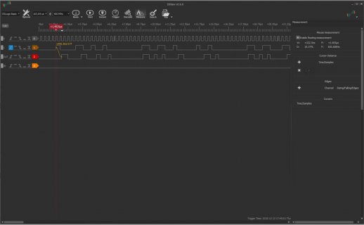
Here is the screenshot of the ~700ns latency that is killing me, LOL.
Timing02.jpg

There is nothing in the loop section. I was externally triggering the interrupt pin. I didn't want there to be anything potentially slowing down the system's ability to respond to an interrupt while I was taking measurements of its latency. I have put the code with the attachinterrupt and the function it calls here:

Code:
#define Data0 2
#define Data7 9
#define ADR0 31
#define ADR7 38
#define ADR8 14
#define ADR14 20
#define OE 22
#define CS 21
#define WRITE_EN 23
#define SWITCH 10


unsigned int integerValue=0;
char incomingByte;
int progaddress = 0;
//int progdata = 0;

void setAddress(int address) {
  uint8_t xlow = address & 0xff;
  uint8_t xhigh = (address >>8);
  for (int pin = ADR0; pin <= ADR7; pin += 1) { //sets output pins with data bits
    digitalWriteFast(pin, xlow & 1);
    xlow = xlow >> 1;
  }
  for (int pin = ADR8; pin <= ADR14; pin += 1) { //sets output pins with data bits
    digitalWriteFast(pin, xhigh & 1);
    xhigh = xhigh >> 1;
  }
}

byte readEPROM(int address) {
  for (int pin = Data0; pin <= Data7; pin += 1) { //set ardino data pins to read
    pinMode(pin, INPUT);
  }
  setAddress(address); // call to sub to set the address bits
  byte data = 0;
  digitalWriteFast(SWITCH, HIGH);
  digitalWriteFast(CS, LOW); //Turns the SRAM ON
  digitalWriteFast(OE, LOW); // SRAM OE ON
  for (int pin = Data7; pin >= Data0; pin -= 1) { // reads data on SRAM outputs into Arduino
    data = (data << 1) + digitalReadFast(pin);
  }
  digitalWriteFast(OE, HIGH); //disables SRAM data outputs
  digitalWriteFast(CS, HIGH); //Turns off the SRAM
  digitalWriteFast(SWITCH, LOW);
  return data;
}

void writeEPROM(int address, byte data) {
  digitalWrite(CS, LOW); //Turns SRAM ON
  digitalWrite(OE, HIGH); //Output Enable OFF
  setAddress(address); 
  for (int pin = Data0; pin <= Data7; pin += 1) { //sets data pins on arduino to OUTPUT mode
    pinMode(pin, OUTPUT);
  }  
  for (int pin = Data0; pin <= Data7; pin += 1) { //sets output pins with data bits
    digitalWrite(pin, data & 1);
    data = data >> 1;
  }
  digitalWriteFast(SWITCH, HIGH);
  digitalWriteFast(WRITE_EN, LOW); //pulls the SRAM W line low for a moment to program the data
  digitalWriteFast(WRITE_EN, LOW); //pulls the SRAM W line low for a moment to program the data
//  digitalWriteFast(WRITE_EN, LOW); //pulls the SRAM W line low for a moment to program the data
  digitalWriteFast(WRITE_EN, LOW); //pulls the SRAM W line low for a moment to program the data
  digitalWriteFast(WRITE_EN, HIGH);
  digitalWriteFast(SWITCH, LOW);
  digitalWriteFast(CS, HIGH);
  for (int pin = Data0; pin <= Data7; pin += 1) { //sets data pins on arduino to INPUT mode
    pinMode(pin, INPUT);
  }  
}

void setup() {
  Serial.begin(9600);
  
  pinMode(CS, OUTPUT);
  digitalWrite(CS, HIGH);
  
  pinMode(OE, OUTPUT);
  digitalWrite(OE, HIGH); //SRAM output enable pin.  HIGH = disabled
  
  pinMode(WRITE_EN, OUTPUT);
  digitalWrite(WRITE_EN, HIGH); // SRAM WRITE PIN
  
  pinMode(SWITCH, OUTPUT);
  digitalWrite(SWITCH, LOW);

  for (int pin = Data0; pin <= Data7; pin += 1) { //set ardino data pins to read
    pinMode(pin, INPUT);
  }
  for (int pin = ADR0; pin <= ADR7; pin += 1) { //sets address pins on arduino to OUTPUT mode
      pinMode(pin, OUTPUT);
  } 
  for (int pin = ADR8; pin <= ADR14; pin += 1) { //sets address pins on arduino to OUTPUT mode
      pinMode(pin, OUTPUT);
  }
  pinMode(29, OUTPUT);
  digitalWriteFast(29, LOW);
  pinMode(30, INPUT);
  attachInterrupt(digitalPinToInterrupt(30), pulse, RISING);
  //NVIC_SET_PRIORITY(IRQ_PORTB, 0);  <This actually SLOWS the latency response!!
}

void pulse(){
  digitalWrite(29, HIGH);
  }

void loop() {
 
Last edited:
I was only calling attachinterrupt once in setup.
So why is it's speed an issue?

I edited the first post code section to reflect what exactly I was doing
I still don't see an attachInterrupt in your code. In setup you only call Serial.begin, digitalWrite and pinMode.

Please post the exact code (all of it) that you are using, in a new message.

Pete
 
some thoughts:
- use always digitalWriteFast()
- use FASTRUN for pulse()
Code:
FASTRUN void pulse(){
  digitalWriteFast(29, HIGH);
  }

NVIC_SET_PRIORITY(IRQ_PORTB, 0); is the highest priority - it will not slow down the response - how do you measure?
If the above code is still to slow, yes, there is a way to make it a little bit faster - if you write your own pin interrupt code. but first, try without.
 
...looking at the code again.. EventResponder::runFromYield(), called in yield(), which runs in loop() disables interrupts.
So, it may help to rewrite your loop for more consistent results:
Code:
void loop() {
 while(1);
}

or overwrite yield:
void yield(void) {};
 
Here is the response using FASTRUN void pulse(): (It is faster than previously BUT it is still taking some 442ns for the interrupt to output. This isn't fast enough. I need this response to be down to no more than ~220ns.

You asked how I am measuring the response time - I am using an scope to see how the NVIC setting is changing the latency. With it off it takes 442ns for the interrupt to trigger the output pin. With it on, it is taking about 450ns. A very small difference but it is there and in the wrong direction, LOL.

timing-442ns.jpg
 
So why is it's speed an issue?


I still don't see an attachInterrupt in your code. In setup you only call Serial.begin, digitalWrite and pinMode.

Please post the exact code (all of it) that you are using, in a new message.

Pete

I think you may have misunderstood what I meant by I'm only calling it once in setup. I am setting up the attachinterrupt in the setup() section only once, which is all it needs to be configured. Speed is an issue because I only have about a 300ns window of time to perform a read/write function in the NVSRAM when the 6303 isn't accessing the NVSRAM.... and ~50ns of that time needs to be available for the actual read/write process... this is why speed is an issue; I need a 250ns or shorter interrupt latency to make this all work.
 
Well, then you need to write your own low-level interrupt, and use the int-vector directly. the yield() issue still remains, so overwrite it.
Take a look to the teensyduino-core, or ask me @weekend.. dunno if your goal is doable, but we can try it :)
 
Not sure of activity on other pins on PORTB … Wondering if the IRQ_PORTB is just getting too much extra activity? Does any change on a PORTB pin trigger the interrupt to parse for Attached Int? That is getting called to parse out the requested pin only to find it wasn't the PIN_30 RISING and then exits. That might explain why NVIC PRI of Zero makes it worse as more ignorable changes will get processed?

With Data0...Data7 for sequential pins being #2 to #9 that uses PORT D, A and C then other pins from PORTB elsewhere.

Perhaps moving PIN_30 to an otherwise unused Port - or shuffling other pins as needed to make one clear?
 
Well, then you need to write your own low-level interrupt, and use the int-vector directly. the yield() issue still remains, so overwrite it.
Take a look to the teensyduino-core, or ask me @weekend.. dunno if your goal is doable, but we can try it :)

This guy was doing it and was seeing very acceptable interrupt latency. Doesn't look like a terribly complex bit of code either but it is a bit beyond my ability.
https://forum.pjrc.com/threads/45413...sy-3-1-and-3-6

He is using pin 14 and 16 here in his example. How would I go about manipulating this code for my application? He was getting down into the 130ns interrupt latencies with this code.

Code:
// teensy 3 FTM timer and isr latency  with scope pin 16 and 14


volatile unsigned long ticks;

FASTRUN void ftm1_isr(void) {
  digitalWriteFast(14, HIGH);
  FTM1_SC &= ~FTM_SC_TOF;  // reset interrupt
  ticks = 1;
}


void init_pwm(int khz) {
  CORE_PIN16_CONFIG = PORT_PCR_MUX(3) | PORT_PCR_DSE | PORT_PCR_SRE; // enable PWM
  //  enabled by init SIM_SCGC6 |= SIM_SCGC6_FTM1;
  // FTM1_CnSC set by init
  NVIC_ENABLE_IRQ(IRQ_FTM1);
  FTM1_SC = 0;
  FTM1_CNT = 0;
  FTM1_MOD = (F_BUS / 1000) / khz - 1;
  FTM1_C0V = (F_BUS / 3000) / khz - 1;
  FTM1_SC = FTM_SC_CLKS(1) | FTM_SC_PS(0) | FTM_SC_TOF | FTM_SC_TOIE;
}

void setup() {
  pinMode(14, OUTPUT);
  init_pwm(40);    // pwm freq in khz on pin 16
  spin();
}

FASTRUN void spin() {
  while (1) {
    if (ticks) {
      digitalWriteFast(14, 0);
      ticks = 0;
    }
  }
}

void loop() {}
 
That is triggered by an internal timer interrupt - not an external pin change. So there is 1 to 1 mapping and a direct call to the code - not call to code that calls code for registered _isr.

As FrankB noted you could rewrite the IRQ_PORTB possible to get to desired code faster - but it will still need to check for desired condition on the desired pin, or exit … re: Post #10

Question: The Pin_30 RISING. Is there another event that happens some repeatable time before that happens? That I assume is when the other processor is done? If there were a signal that always preceded that it would give more time to react.
 
I am setting up the attachinterrupt in the setup() section only once, which is all it needs to be configured
Yes, I see that now. But in your first message, with your comment about attachInterrupt being horrifically slow, I thought you might be doing what I have seen in some Arduino threads where the user does a detachInterrupt and then an attachInterrupt in the interrupt routine itself. That's why I wanted to see where you were doing the attachInterrupt.

As an aside: did you edit your message #3 and add the code to it later? I could've sworn there was no code in that message when I replied in #4.

Pete
 
This guy was doing it and was seeing very acceptable interrupt latency. Doesn't look like a terribly complex bit of code either but it is a bit beyond my ability.
https://forum.pjrc.com/threads/45413...sy-3-1-and-3-6

He is using pin 14 and 16 here in his example. How would I go about manipulating this code for my application? He was getting down into the 130ns interrupt latencies with this code.

Code:
// teensy 3 FTM timer and isr latency  with scope pin 16 and 14


volatile unsigned long ticks;

FASTRUN void ftm1_isr(void) {
  digitalWriteFast(14, HIGH);
  FTM1_SC &= ~FTM_SC_TOF;  // reset interrupt
  ticks = 1;
}


void init_pwm(int khz) {
  CORE_PIN16_CONFIG = PORT_PCR_MUX(3) | PORT_PCR_DSE | PORT_PCR_SRE; // enable PWM
  //  enabled by init SIM_SCGC6 |= SIM_SCGC6_FTM1;
  // FTM1_CnSC set by init
  NVIC_ENABLE_IRQ(IRQ_FTM1);
  FTM1_SC = 0;
  FTM1_CNT = 0;
  FTM1_MOD = (F_BUS / 1000) / khz - 1;
  FTM1_C0V = (F_BUS / 3000) / khz - 1;
  FTM1_SC = FTM_SC_CLKS(1) | FTM_SC_PS(0) | FTM_SC_TOF | FTM_SC_TOIE;
}

void setup() {
  pinMode(14, OUTPUT);
  init_pwm(40);    // pwm freq in khz on pin 16
  spin();
}

FASTRUN void spin() {
  while (1) {
    if (ticks) {
      digitalWriteFast(14, 0);
      ticks = 0;
    }
  }
}

void loop() {}

Ah, I didn't quite understand what he was actually doing then. When I saw the scope shot it looked like he generated a pulse into an interrupt pin and then within that 130ns timeframe, the MCU handled the interrupt and set a different pin to a HIGH state output.

This is a very fast MCU and I think this latency is just a result of the "generalized" interrupt handling routines that are in place. There has to be a way to modify that back-end code, I would imagine. From what Frank B stated a few posts above, that sounds exactly like what I need to do here. I just am not sure how to go about doing that. Any guidance you could offer here? :)
 
@AshPowers - I just wrote a sketch to see that per POSTS #10 and #12 any change on PORT_B triggers the interrupt handler, as it must to then determine is a requested pin change interrupt has occurred.

If there is other 'noise' on PORTB - it will trigger the base interrupt each time there is any pin change for the code to examine. That could be queueing multiple interrupts in progress before the actual pin #30 change happens.

<EDIT>:: CORRECTION - I have finished writing the test - other pins on the port do NOT seem to trigger the interrupt handler.
 
Last edited:
Well, then you need to write your own low-level interrupt, and use the int-vector directly. the yield() issue still remains, so overwrite it.
Take a look to the teensyduino-core, or ask me @weekend.. dunno if your goal is doable, but we can try it :)

Hi Frank!

Well, the fastest I can get it down to using the attachinterrupt, FASTRUN function, and digitalwritefast to set the output pin, is ~450ns.

I really need to get this down into the 250ns maximum to be able to squeeze everything in.

How can one go about doing this?
Thanks!
 
@AshPowers - I just wrote a sketch to see that per POSTS #10 and #12 any change on PORT_B triggers the interrupt handler, as it must to then determine is a requested pin change interrupt has occurred.

If there is other 'noise' on PORTB - it will trigger the base interrupt each time there is any pin change for the code to examine. That could be queueing multiple interrupts in progress before the actual pin #30 change happens.

<EDIT>:: CORRECTION - I have finished writing the test - other pins on the port do NOT seem to trigger the interrupt handler.

I changed all the pins around to free up PortA for the interrupt, pin 39, PTA17. Everything else is on all other ports. Even doing this and using the NVIC priority for port A set to zer0,, it makes virtually difference. Should I be reserving a specific port to use for interrupts? Is any one of them faster than the rest?

I overclocked the processor and am able to get the latency down to around 350ns but I'm still about 150ns away from being able to make this work. :-(

PORTC appears to only have 12 pins. Perhaps this is a better port to use as the interrupt handler will have fewer lines to check?

Code:
#define Data0 A0
#define Data7 A7
#define ADR0 0
#define ADR1 1
#define ADR2 2
#define ADR3 5
#define ADR4 6
#define ADR5 7
#define ADR6 8
#define ADR7 9
#define ADR8 10
#define ADR9 11
#define ADR10 12
#define ADR11 29
#define ADR12 30
#define ADR13 31
#define ADR14 32

#define OE 33
#define CS 34
#define WRITE_EN 35
#define SWITCH 36

#define PTC10 37
#define PTC11 38
#define PTA17 39  // <--  This is the new interrupt input pin
 
Not sure if this is valid or accurate or complete - but from my test code use this to trigger your _isr for a quick test:

Code:
FASTRUN void pulse(){
  digitalWrite(29, HIGH);
  }

// original vector
void (*prevInterruptPtr)(void);

void setup() {
// ...
  attachInterrupt( 39, pulse, RISING);
  prevInterruptPtr = _VectorsRam[IRQ_PORTA + 16]; // this saves the original vector
  attachInterruptVector(IRQ_PORTA, pulse );

  //NVIC_SET_PRIORITY(IRQ_PORTA, 0);

  // Writing to the SCB_SHPR3 register to lower the Systick priority
  SCB_SHPR3 = 0x20200000;  // Systick = priority 32 (defaults to zero)

// ...
}

I will check this Saturday. Unfortunately I made a careless mistake and the scope terminal to the chip select line came loose and the CS line touched a 12V rail in the engine computer - blew three of the analog switches and blew about half of the IO ports on the T3.5. :'-( I ordered another T3.5 and have a bunch of switches - gotta love Amazon! Hah! Fortunately the NVSRAM appears to be functioning properly.
"Prototyping: It'll be fun, they said.."
 
Ick - Prototyping … it CAN be fun … or just an adventure.

My prior post will probably hang - as the replacement _isr code doesn't clear the interrupt on exit? I just tried a variant and my working sample with the PJRC pin search and call working as follows.

I have a sample running on T_3.5 and T_3.6 with loop() - now just a while(1) where each cycle writes either 1 or 0 to a pin triggering a rising interrupt - with a jumper pin #30 to #32 that increments a counter, and toggles the LED pin.

The T_3.5 at 168 MHz with 56 MHz F_bus gets about 1119000 cycles per second, where second is tracked by the cycle counter.
The T_3.6 at 256 MHz with 128 MHz F_bus gets about 1945600 cycles per second, where second is tracked by the cycle counter.
The T_3.6 at 256 MHz with 64 MHz F_bus gets about 1660000 cycles per second, where second is tracked by the cycle counter.

So this code with little overhead and not much left for anything else but servicing the interrupt on an OC'd T_3.5 looks to be taking some part of 894 ns for the _isr with one part each write 1 and write 0 since the processor is doing it's own triggering.

256 OC'd T_3.6 case now generates 2097065 toggles with the bool added and using PTOR to toggle LED.

<edit>: Above was default FASTER optimize - just went FASTEST+pure,w/LTO and the T_3.6 is doing 2264025 and the T_3.5 now doing 1433804/sec with compile and code changes.

I used Cycle Counter to watch the second pass because it is less overhead than micros - and it may miss a few ticks.

FWIW here's the code in case it shows something that could be better done or tested with.
With a scope the time between pin 30 (w/jumper to 32) going high and LED pin 13 toggle will show the delay in the _isr():
Code:
#define Tst_b19 30
#define Tst_b11 32

uint32_t PBcnt_ii = 0;
FASTRUN void Pin_isr(void) {
  PBcnt_ii++;
  GPIOC_PTOR = 32; // digitalWriteFast(13, !digitalReadFast(13));
}

uint32_t OutWait;
void setup() {
  pinMode(13, OUTPUT);
  Serial1.begin(9600);
  while (!Serial && millis() < 5000 );
  Serial.println("\n" __FILE__ " " __DATE__ " " __TIME__);

  pinMode(Tst_b19, INPUT);
  pinMode(Tst_b11, OUTPUT);
  attachInterrupt(Tst_b19, Pin_isr, RISING);
  NVIC_SET_PRIORITY(IRQ_PORTB, 0);
  // Writing to the SCB_SHPR3 register to lower the Systick priority
  SCB_SHPR3 = 0x20200000;  // Systick = priority 32 (defaults to zero)

  // Enable CPU Cycle Counter - if desired for time base
  ARM_DEMCR |= ARM_DEMCR_TRCENA;
  ARM_DWT_CTRL |= ARM_DWT_CTRL_CYCCNTENA;

  while (!Serial && millis() < 5000 );
  Serial.println("\n" __FILE__ " " __DATE__ " " __TIME__);
  Serial.print("\nCPU=" );
  Serial.print(F_CPU);
  Serial.print("\nBUS=");
  Serial.println(F_BUS);
  digitalWriteFast( Tst_b11, 1 );
  OutWait = ARM_DWT_CYCCNT;
}

uint32_t ii = 0;
uint32_t PBcnt_iiH = 0;
bool dotog=false;
void loop() {
  while (1) {
    ii++;
    if ( (ARM_DWT_CYCCNT - OutWait) > F_CPU) {
      Serial.print("PBcnt_ii =");
      Serial.println( PBcnt_ii );
      PBcnt_ii = 0;
      OutWait = ARM_DWT_CYCCNT;
    }
//    if ( PBcnt_iiH != PBcnt_ii ) {
    if ( (dotog = !dotog) ) {
      digitalWriteFast( Tst_b11, 0 );
      PBcnt_iiH = PBcnt_ii;
    }
    else {
      digitalWriteFast( Tst_b11, 1 );
    }
  }
}

<edit> :: BTW Frank_B - you can see above that changing the F_BUS allows faster access and change to the GPIO pins. Those are serviced at F_BUS speeds ( this relates to that other thread where I didn't comment because I wanted to see it again first … this does that as the 68 MHz F_BUS give 2173968 compiled the same as the 128 MHz F_BUS giving 2264025 - though the GAP shown above before latest changes is closed a bit!
 
Last edited:
Ick - Prototyping … it CAN be fun … or just an adventure.

My prior post will probably hang - as the replacement _isr code doesn't clear the interrupt on exit? I just tried a variant and my working sample with the PJRC pin search and call working as follows.

I have a sample running on T_3.5 and T_3.6 with loop() - now just a while(1) where each cycle writes either 1 or 0 to a pin triggering a rising interrupt - with a jumper pin #30 to #32 that increments a counter, and toggles the LED pin.

The T_3.5 at 168 MHz with 56 MHz F_bus gets about 1119000 cycles per second, where second is tracked by the cycle counter.
The T_3.6 at 256 MHz with 128 MHz F_bus gets about 1945600 cycles per second, where second is tracked by the cycle counter.
The T_3.6 at 256 MHz with 64 MHz F_bus gets about 1660000 cycles per second, where second is tracked by the cycle counter.

So this code with little overhead and not much left for anything else but servicing the interrupt on an OC'd T_3.5 looks to be taking some part of 894 ns for the _isr with one part each write 1 and write 0 since the processor is doing it's own triggering.

256 OC'd T_3.6 case now generates 2097065 toggles with the bool added and using PTOR to toggle LED.

<edit>: Above was default FASTER optimize - just went FASTEST+pure,w/LTO and the T_3.6 is doing 2264025 and the T_3.5 now doing 1433804/sec with compile and code changes.

I used Cycle Counter to watch the second pass because it is less overhead than micros - and it may miss a few ticks.

FWIW here's the code in case it shows something that could be better done or tested with.
With a scope the time between pin 30 (w/jumper to 32) going high and LED pin 13 toggle will show the delay in the _isr():

If I understand your numbers there, it sounds like you are seeing some 600ns latency?

Just before I blew this thing up last night I was able to get the latency down from pin input to pin output to about 350ns by overclocking the processor and changing the compiler to Fastest + purecode with LTO. I have no idea what purecode and LTO is, or what kind of optimizations are being made during compile time that provide these differing speeds. I *literally* just got into programming these little microcontrollers about two weeks ago.

It seems to me that at a lower level in the coding for these MCUs, one could modify the existing ISR routine to look at just ONE specific pin on a given port rather than polling through each pin on each port which is what I gather is going on from explanations I've read about this subject. This "generalized" ISR handler works fine for guys wanting to turn a light on or something to that effect, but for applications like what I am doing that require significantly better response time, that generic back end code just doesn't cut it.

I'd really like to learn more about how these IRQs work on the back end so I Can better wrap my mind around it. I have a lot of time on my hands to figure this out - I just need some minor direction to be pointed in. :)
 
That '697 ns' on the T_3.5 is showing total cycle time :: same Teensy doing output -- that triggers input Rising -- then dropping the trigger and repeating. So running that code on a Scope would show the response time of the _isr.

I just got a Logic Analyzer - but don't have time just now to hook it up to post a picture. As noted the LED toggles the _isr so scope seeing the jumpered line rise until the LED goes up/down would represent some sense of what the code above has for just that portion.

Is there any preceding electrical event to the RISE of the pin you want to see? Is there some other data ready signal the other processor sees before it completes and raises the pin you want to monitor that would buy you more time to respond?

The Tools / Optimize choices are 'generally' as labelled where the compiler expects to get faster code - but that isn't always the case as some optimizations may have bad side effects to the app in use, like growing code to be faster - but larger code overfills the cache causing slower access on the MCU in the end.

OK, tomorrow when the replacement T3.5 shows up I will load up your code and my scope to see what kind of latency it produces.

As for the signaling, there is no other electrical event preceding the rise of the chip enable line to tell me that the processor is about to make the EPROM port available for external reads/writes... at least, none that I am aware of. I've got the entire read or write cycle to the NVSRAM down right at 45ns and am able to get stable reads/writes at that interval.

What I will need the code to do is if there is a read or write command issued by the 3rd computer connected to the T3.5's USB port, the T3.5 will setup the address and data lines and then hold until the interrupt triggers the next step to throw the analog switches, connecting the T3.5 to the NVRAM. I've found that with this NVRAM, if the address, data, CE, OE, and or the WE pins are all set prior to throwing the switches to connect the T3.5 to the NVSRAM, simply throwing the switches for 45ns and then throwing them back to the 6303, the NVSRAM is plenty happy with shot-gunning all of the lines like that.... rather than having to sequence CE, OE/WE in an order. This makes the read/write very efficient.

My only concern is if the actual code handling this is going to introduce more latency of it's own. The function that gets called on the interrupt will be cycling along with the CE signal which is OK, but in the function itself it will need to determine if a read or write is to be performed. I'm thinking that this function only needs like four lines of code. One to check if a read or write request has been made and if so, throw the analog switches for 45ns, and then back. Then finally it needs to be able to tell the readEPROM or writeEPROM function (which will be holding for the interrupt), that the switches have been toggled and that they can move on through the rest of their code.

The main question is how many clock cycles will that first line of code in the interrupt function take (where it checks to see if the readEPROM or writeEPROM function has been queued)..

Or perhaps there is another more clever way of programming that will be faster.?

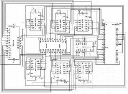
Here's a shot of my schematic just for reference.
circuit01.jpg

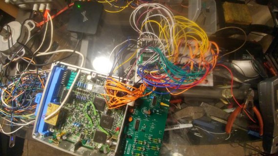
And a pic of the prototype (missing the T3.5 in the top right which went critical mass :'-(
circuit02.jpg
 
Last edited:
Sounds like a lot of code to run conditionally.

Somebody posted this earlier and results show a T_3.6 at 256 MHz responding to a timer executing and timing a few instructions:: Very-Fast-Interval-Timer

If I'm reading the output right it is 13 Cycles to do this - to leave the reset code at 0 clocks and read the .ticks showing 13 clocks before storing it:
Code:
  CycleCount.reset();

  if (SampleIndex < nSamples)
  {
    SampleTimes[SampleIndex] = Count;
    ProcessingTimes[SampleIndex] = CycleCount.ticks();

And the timer is making that happen 1 million times/sec and the full loop takes ~255 - cycles - meaning about nothing left if I'm reading it right given 256,000,000 cycles per second.
 
Status
Not open for further replies.
Back
Top