Here's some example code... this shifts out data in parallel to pins 10-13 every 25 ns. It requires KurtE's FlexIO_t4 library (https://github.com/KurtE/FlexIO_t4). (Note that there's a typo in that library that needs to be fixed before this will compile: In FlexIO_t4.cpp, the initialization for "flex2_hardware" needs an ampersand before "IRQHandler_FlexIO2" to match the one for "flex1_hardware".)
Code:
// Transfer data from dataBuffer to FlexIO
// FlexIO hardware shifts out 4 bits at a time
#include <Arduino.h>
#include "FlexIO_t4.h"
#include "DMAChannel.h"
FlexIOHandler *pFlex;
IMXRT_FLEXIO_t *p;
const FlexIOHandler::FLEXIO_Hardware_t *hw;
DMAChannel myDMA;
volatile uint32_t DMAMEM dataBuffer[2] __attribute__((aligned(32)));
void setup() {
Serial.begin(115200);
delay(1000);
Serial.println("Start setup");
delay(1000);
/* Get a FlexIO channel */
pFlex = FlexIOHandler::flexIOHandler_list[1]; // use FlexIO2
/* Pointer to the port structure in the FlexIO channel */
p = &pFlex->port();
/* Pointer to the hardware structure in the FlexIO channel */
hw = &pFlex->hardware();
/* Basic pin setup */
pinMode(10, OUTPUT); // FlexIO2:0
pinMode(12, OUTPUT); // FlexIO2:1
pinMode(11, OUTPUT); // FlexIO2:2
pinMode(13, OUTPUT); // FlexIO2:3
/* High speed and drive strength configuration */
*(portControlRegister(10)) = 0xFF;
*(portControlRegister(12)) = 0xFF;
*(portControlRegister(11)) = 0xFF;
*(portControlRegister(13)) = 0xFF;
/* Set clock */
pFlex->setClockSettings(3, 0, 0); // 480 MHz
/* Set up pin mux */
pFlex->setIOPinToFlexMode(10);
pFlex->setIOPinToFlexMode(12);
pFlex->setIOPinToFlexMode(11);
pFlex->setIOPinToFlexMode(13);
/* Enable the clock */
hw->clock_gate_register |= hw->clock_gate_mask;
/* Enable the FlexIO with fast access */
p->CTRL = FLEXIO_CTRL_FLEXEN | FLEXIO_CTRL_FASTACC;
/* Shifter 0 registers */
#define S0_PWIDTH 3 // 4-bit parallel shift width
#define S0_INSRC 1 // Input source from Shifter 1
#define S0_SSTOP 0 // Stop bit disabled
#define S0_SSTART 0 // Start bit disabled, transmitter loads data on enable
#define S0_TIMSEL 0 // Use timer 0
#define S0_TIMPOL 1 // Shift on negedge of clock
#define S0_PINCFG 3 // Shifter pin output
#define S0_PINSEL 0 // Select pins FXIO_D0 through FXIO_D3
#define S0_PINPOL 0 // Shifter pin active high polarity
#define S0_SMOD 2 // Shifter transmit mode
p->SHIFTCFG[0] = (S0_PWIDTH<<16) | (S0_INSRC<<8) | (S0_SSTOP<<4) | (S0_SSTART<<0);
p->SHIFTCTL[0] = (S0_TIMSEL<<24) | (S0_TIMPOL<<23) | (S0_PINCFG<<16) | (S0_PINSEL<<8) | (S0_PINPOL<<7) | (S0_SMOD<<0);
/* Timer 0 registers */
#define T0_TIMOUT 1 // Timer output is logic zero when enabled and is not affected by the Timer reset
#define T0_TIMDEC 0 // Timer decrements on FlexIO clock, shift clock equals timer output
#define T0_TIMRST 0 // Timer never reset
#define T0_TIMDIS 2 // Timer disabled on Timer compare
#define T0_TIMENA 2 // Timer enabled on Trigger high
#define T0_TSTOP 0 // Stop bit disabled
#define T0_TSTART 0 // Start bit disabled
#define T0_TRGSEL (4*0+1) // Trigger select Shifter 0 status flag
#define T0_TRGPOL 1 // Trigger active low
#define T0_TRGSRC 1 // Internal trigger selected
#define T0_PINCFG 0 // Timer pin output disabled
#define T0_PINSEL 0 // Select pin FXIO_D0
#define T0_PINPOL 0 // Timer pin polarity active high
#define T0_TIMOD 1 // Dual 8-bit counters baud mode
p->TIMCFG[0] = (T0_TIMOUT<<24) | (T0_TIMDEC<<20) | (T0_TIMRST<<16) | (T0_TIMDIS<<12) | (T0_TIMENA<<8) | (T0_TSTOP<<4) | (T0_TSTART<<1);
p->TIMCTL[0] = (T0_TRGSEL<<24) | (T0_TRGPOL<<23) | (T0_TRGSRC<<22) | (T0_PINCFG<<16) | (T0_PINSEL<<8) | (T0_PINPOL<<7) | (T0_TIMOD<<0);
#define CLOCK_DIVIDER 6 // Shift clock frequency is 6 times slower than FlexIO clock = 80 MHz (12.5 ns width from positive to negative edge, 25 ns between shifts)
#define SHIFTS_PER_TRANSFER 8 // Shift out 8 times with every transfer = one 32-bit word = contents of Shifter 0
p->TIMCMP[0] = ((SHIFTS_PER_TRANSFER*2-1)<<8) | ((CLOCK_DIVIDER-1)<<0);
Serial.println("FlexIO setup complete");
Serial.println("Start DMA setup");
/* Enable DMA trigger on Shifter 0 */
p->SHIFTSDEN |= (1<<0); // DMA request is generated when data is transferred from buffer0 to shifter0
/* Disable DMA channel so it doesn't start transferring yet */
myDMA.disable();
/* Configure DMA to transfer 32-bit words from dataBuffer to Shifter 0 buffer */
unsigned int transferBytes = sizeof(dataBuffer);
myDMA.sourceBuffer(&(dataBuffer[0]), transferBytes); // transfer entire dataBuffer
myDMA.destination(p->SHIFTBUF[0]);
/* Set DMA channel to automatically disable on completion (we have to manually enable it every loop) */
myDMA.disableOnCompletion();
/* Set up DMA channel to use Shifter 0 trigger */
myDMA.triggerAtHardwareEvent(hw->shifters_dma_channel[0]);
Serial.println("DMA setup complete");
/* initialize data buffer */
dataBuffer[0] = (0<<0) | (1<<4) | (2<<8) | (3<<12) | (4<<16) | (5<<20) | (6<<24) | (7<<28);
dataBuffer[1] = (8<<0) | (9<<4) | (10<<8) | (11<<12) | (12<<16) | (13<<20) | (14<<24) | (15<<28);
/* flush DMAMEM cache */
arm_dcache_flush((void*)dataBuffer, sizeof(dataBuffer));
}
void loop() {
myDMA.enable();
// DMA transfer and FlexIO shifts happen in background, no CPU involvement
delay(4000);
}
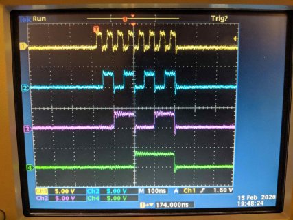
Here's an oscilloscope screenshot with channels 1,2,3,4 hooked to pins 10,12,11,13: