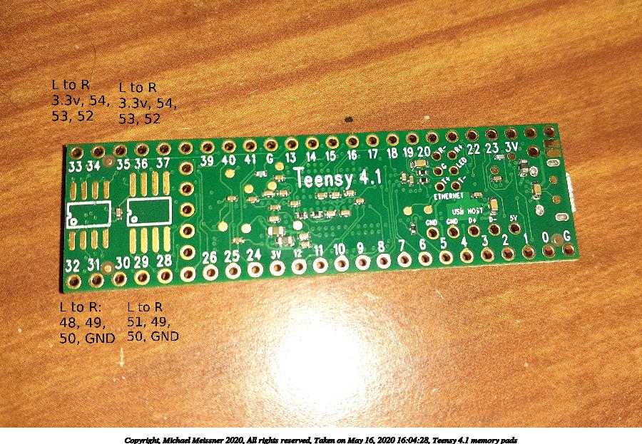
On the bottom psram pads, between outer pins 32 and 30, the bottom 4 pads are, going left to right are:
- Pad 48 (CS pin)
- Pad 49
- Pad 50
- Ground
On the bottom psram pads, between outer pins 32 and 30, the top pads, going left to right are:
- 3.3v
- Pad 54
- Pad 53
- Pad 52
On the Flash pads between outer pins 30 and 28, the bottom 4 pads are, going left to right are:
- Pad 51 (CS pin)
- Pad 49
- Pad 50
- Ground
On the Flash pads between outer pins 30 and 28, the top 4 pads are, going left to right are:
- 3.3v
- Pad 54
- Pad 53
- Pad 52
I.e. except for the CS pin, the remaining 7 pads are the same between the two solder areas. The psram and flash chips all have a dot on the chip, and you line that up with the dot on the PCB.
The holes next to the micro-SD card reader, are in the same order as the Teensy 4.0, but in a different location. Going from top to bottom on the above picture of the back side, the pins are:
- Pin 38 on the outer row
- On/off
- Program
- Ground
- 3.3v
- Vbat
- Pin 27 on the outer row
The pins for the USB host are labeled on the PCB (i.e. ground, ground, D+, D-, 5v).
I'm not sure the ethernet pins have names.

") And I haven't yet attempted to exercise the SPIFFS with latest 1.52 core ...
And I haven't yet attempted to exercise the SPIFFS with latest 1.52 core ...