Problem trying to read OV7670 camera under IRQ Teensy 4.0

Status
Not open for further replies.
Right now it looks like my Wire(I2) connection is actually not working to that one... So may need to rework... Scanner is not finding it. :eek:

The read from other software on other camera
Code:
I2C Read: reg: 0x00(GAIN), value = 0x7F
I2C Read: reg: 0x01(BLUE), value = 0xF0
I2C Read: reg: 0x02(RED), value = 0x40
I2C Read: reg: 0x03(VREF), value = 0xA
I2C Read: reg: 0x04(COM1), value = 0x0
I2C Read: reg: 0x05(BAVE), value = 0x2F
I2C Read: reg: 0x06(GbAVE), value = 0x40
I2C Read: reg: 0x07(AECHH), value = 0x40
I2C Read: reg: 0x08(RAVE), value = 0x36
I2C Read: reg: 0x09(COM2), value = 0x1
I2C Read: reg: 0x0a(PID), value = 0x76
I2C Read: reg: 0x0b(VER), value = 0x73
I2C Read: reg: 0x0c(COM3), value = 0x0
I2C Read: reg: 0x0d(COM4), value = 0x40
I2C Read: reg: 0x0e(COM5), value = 0x61
I2C Read: reg: 0x0f(COM6), value = 0x4B
I2C Read: reg: 0x10(AECH), value = 0x72
I2C Read: reg: 0x11(CLKRC), value = 0x3
I2C Read: reg: 0x12(COM7), value = 0x4
I2C Read: reg: 0x13(COM8), value = 0xE7
I2C Read: reg: 0x14(COM9), value = 0x38
I2C Read: reg: 0x15(COM10), value = 0x20
I2C Read: reg: 0x16(*RSVD*), value = 0x2
I2C Read: reg: 0x17(HSTART), value = 0x13
I2C Read: reg: 0x18(HSTOP), value = 0x1
I2C Read: reg: 0x19(VSTART), value = 0x2
I2C Read: reg: 0x1a(VSTOP), value = 0x7A
I2C Read: reg: 0x1b(PSHFT), value = 0x0
I2C Read: reg: 0x1c(MIDH), value = 0x7F
I2C Read: reg: 0x1d(MIDL), value = 0xA2
I2C Read: reg: 0x1e(MVFP), value = 0x7
I2C Read: reg: 0x1f(LAEC), value = 0x0
I2C Read: reg: 0x20(ADCCTR0), value = 0x4
I2C Read: reg: 0x21(ADCCTR1), value = 0x2
I2C Read: reg: 0x22(ADCCTR2), value = 0x91
I2C Read: reg: 0x23(ADCCTR3), value = 0x0
I2C Read: reg: 0x24(AEW), value = 0x95
I2C Read: reg: 0x25(AEB), value = 0x33
I2C Read: reg: 0x26(VPT), value = 0xE3
I2C Read: reg: 0x27(BBIAS), value = 0x80
I2C Read: reg: 0x28(GbBIAS), value = 0x80
I2C Read: reg: 0x29(*RSVD*), value = 0x7
I2C Read: reg: 0x2a(EXHCH), value = 0x0
I2C Read: reg: 0x2b(EXHCL), value = 0x0
I2C Read: reg: 0x2c(RBIAS), value = 0x80
I2C Read: reg: 0x2d(ADVFL), value = 0x0
I2C Read: reg: 0x2e(ADVFH), value = 0x0
I2C Read: reg: 0x2f(YAVE), value = 0x16
I2C Read: reg: 0x30(HSYST), value = 0x8
I2C Read: reg: 0x31(HSYEN), value = 0x30
I2C Read: reg: 0x32(HREF), value = 0xB6
I2C Read: reg: 0x33(CHLF), value = 0xB
I2C Read: reg: 0x34(ARBLM), value = 0x11
I2C Read: reg: 0x35(*RSVD*), value = 0xB
I2C Read: reg: 0x36(*RSVD*), value = 0x0
I2C Read: reg: 0x37(ADC), value = 0x1D
I2C Read: reg: 0x38(ACOM), value = 0x71
I2C Read: reg: 0x39(OFON), value = 0x2A
I2C Read: reg: 0x3a(TSLB), value = 0x4
I2C Read: reg: 0x3b(COM11), value = 0x12
I2C Read: reg: 0x3c(COM12), value = 0x78
I2C Read: reg: 0x3d(COM13), value = 0xC0
I2C Read: reg: 0x3e(COM14), value = 0x0
I2C Read: reg: 0x3f(EDGE), value = 0x1
I2C Read: reg: 0x40(COM15), value = 0x10
I2C Read: reg: 0x41(COM16), value = 0x38
I2C Read: reg: 0x42(COM17), value = 0x0
I2C Read: reg: 0x43(AWBC1), value = 0xA
I2C Read: reg: 0x44(AWBC2), value = 0xF0
I2C Read: reg: 0x45(AWBC3), value = 0x34
I2C Read: reg: 0x46(AWBC4), value = 0x58
I2C Read: reg: 0x47(AWBC5), value = 0x28
I2C Read: reg: 0x48(AWBC6), value = 0x3A
I2C Read: reg: 0x49(*RSVD*), value = 0x0
I2C Read: reg: 0x4a(*RSVD*), value = 0x0
I2C Read: reg: 0x4b(REG4B), value = 0x9
I2C Read: reg: 0x4c(DNSTH), value = 0x20
I2C Read: reg: 0x4d(DM_POS), value = 0x40
I2C Read: reg: 0x4e(*RSVD*), value = 0x20
I2C Read: reg: 0x4f(MTX1), value = 0xB3
I2C Read: reg: 0x50(MTX2), value = 0xB3
I2C Read: reg: 0x51(MTX3), value = 0x0
I2C Read: reg: 0x52(MTX4), value = 0x3D
I2C Read: reg: 0x53(MTX5), value = 0xA7
I2C Read: reg: 0x54(MTX6), value = 0xE4
I2C Read: reg: 0x55(BRIGHT), value = 0x0
I2C Read: reg: 0x56(CONTRAS), value = 0x40
I2C Read: reg: 0x57(CONTRAS_CENTER), value = 0x80
I2C Read: reg: 0x58(MTXS), value = 0x9E
I2C Read: reg: 0x59(AWBC7), value = 0x88
I2C Read: reg: 0x5a(AWBC8), value = 0x88
I2C Read: reg: 0x5b(AWBC9), value = 0x44
I2C Read: reg: 0x5c(AWBC10), value = 0x67
I2C Read: reg: 0x5d(AWBC11), value = 0x49
I2C Read: reg: 0x5e(AWBC12), value = 0xE
I2C Read: reg: 0x5f(B_LMT), value = 0xF0
I2C Read: reg: 0x60(R_LMT), value = 0xF0
I2C Read: reg: 0x61(G_LMT), value = 0xF0
I2C Read: reg: 0x62(LCC1), value = 0x0
I2C Read: reg: 0x63(LCC2), value = 0x0
I2C Read: reg: 0x64(LCC3), value = 0x50
I2C Read: reg: 0x65(LCC4), value = 0x30
I2C Read: reg: 0x66(LCC5), value = 0x0
I2C Read: reg: 0x67(MANU), value = 0x80
I2C Read: reg: 0x68(MANV), value = 0x80
I2C Read: reg: 0x69(GFIX), value = 0x0
I2C Read: reg: 0x6a(GGAIN), value = 0x6C
I2C Read: reg: 0x6b(DBLV), value = 0x4A
I2C Read: reg: 0x6c(AWBCTR3), value = 0xA
I2C Read: reg: 0x6d(AWBCTR2), value = 0x55
I2C Read: reg: 0x6e(AWBCTR1), value = 0x11
I2C Read: reg: 0x6f(AWBCTR0), value = 0x9F
I2C Read: reg: 0x70(SCALING_XSC), value = 0x3A
I2C Read: reg: 0x71(SCALING_YSC), value = 0x35
I2C Read: reg: 0x72(SCALING_DCWCTR), value = 0x11
I2C Read: reg: 0x73(SCALING_PCLK_DIV), value = 0xF0
I2C Read: reg: 0x74(REG74), value = 0x10
I2C Read: reg: 0x75(REG75), value = 0x5
I2C Read: reg: 0x76(REG76), value = 0xE1
I2C Read: reg: 0x77(REG77), value = 0x1
I2C Read: reg: 0x78(*RSVD*), value = 0x4
I2C Read: reg: 0x79(*RSVD*), value = 0x26
I2C Read: reg: 0x7a(SLOP), value = 0x20
I2C Read: reg: 0x7b(GAMA1), value = 0x10
I2C Read: reg: 0x7c(GAMA2), value = 0x1E
I2C Read: reg: 0x7d(GAMA3), value = 0x35
I2C Read: reg: 0x7e(GAMA4), value = 0x5A
I2C Read: reg: 0x7f(GAMA5), value = 0x69
I2C Read: reg: 0x80(GAMA6), value = 0x76
I2C Read: reg: 0x81(GAMA7), value = 0x80
I2C Read: reg: 0x82(GAMA8), value = 0x88
I2C Read: reg: 0x83(GAMA9), value = 0x8F
I2C Read: reg: 0x84(GAMA10), value = 0x96
I2C Read: reg: 0x85(GAMA11), value = 0xA3
I2C Read: reg: 0x86(GAMA12), value = 0xAF
I2C Read: reg: 0x87(GAMA13), value = 0xC4
I2C Read: reg: 0x88(GAMA14), value = 0xD7
I2C Read: reg: 0x89(GAMA15), value = 0xE8
I2C Read: reg: 0x8a(*RSVD*), value = 0x0
I2C Read: reg: 0x8b(*RSVD*), value = 0x0
I2C Read: reg: 0x8c(?RGB444), value = 0x0
I2C Read: reg: 0x8d(*RSVD*), value = 0x4F
I2C Read: reg: 0x8e(*RSVD*), value = 0x0
I2C Read: reg: 0x8f(*RSVD*), value = 0x0
I2C Read: reg: 0x90(*RSVD*), value = 0x0
I2C Read: reg: 0x91(*RSVD*), value = 0x0
I2C Read: reg: 0x92(DM_LNL), value = 0x0
I2C Read: reg: 0x93(DM_LNH), value = 0x0
I2C Read: reg: 0x94(LCC6), value = 0x50
I2C Read: reg: 0x95(LCC7), value = 0x50
I2C Read: reg: 0x96(*RSVD*), value = 0x0
I2C Read: reg: 0x97(*RSVD*), value = 0x30
I2C Read: reg: 0x98(*RSVD*), value = 0x20
I2C Read: reg: 0x99(*RSVD*), value = 0x30
I2C Read: reg: 0x9a(*RSVD*), value = 0x84
I2C Read: reg: 0x9b(*RSVD*), value = 0x29
I2C Read: reg: 0x9c(*RSVD*), value = 0x3
I2C Read: reg: 0x9d(BD50ST), value = 0x4C
I2C Read: reg: 0x9e(BD60ST), value = 0x3F
I2C Read: reg: 0x9f(HAECC1), value = 0x78
I2C Read: reg: 0xa0(HAECC2), value = 0x68
I2C Read: reg: 0xa1(DSPC3), value = 0x3
I2C Read: reg: 0xa2(SCALING_PCLK_DELAY), value = 0x2
I2C Read: reg: 0xa3(*RSVD*), value = 0x4
I2C Read: reg: 0xa4(NT_CTRL), value = 0x88
I2C Read: reg: 0xa5(AECGMAX), value = 0x5
I2C Read: reg: 0xa6(LPH), value = 0xD8
I2C Read: reg: 0xa7(UPL), value = 0xD8
I2C Read: reg: 0xa8(TPL), value = 0xF0
I2C Read: reg: 0xa9(TPH), value = 0x90
I2C Read: reg: 0xaa(NALG), value = 0x94
I2C Read: reg: 0xab(*RSVD*), value = 0x7
I2C Read: reg: 0xac(STR-OPT), value = 0x0
I2C Read: reg: 0xad(STR_R), value = 0x80
I2C Read: reg: 0xae(STR_G), value = 0x80
I2C Read: reg: 0xaf(STR_B), value = 0x80
I2C Read: reg: 0xb0(*RSVD*), value = 0x84
I2C Read: reg: 0xb1(ABLC1), value = 0xC
I2C Read: reg: 0xb2(*RSVD*), value = 0xE
I2C Read: reg: 0xb3(THL_ST), value = 0x82
I2C Read: reg: 0xb4(*RSVD*), value = 0x0
I2C Read: reg: 0xb5(THL_DLT), value = 0x4
I2C Read: reg: 0xb6(*RSVD*), value = 0x0
I2C Read: reg: 0xb7(*RSVD*), value = 0x66
I2C Read: reg: 0xb8(*RSVD*), value = 0xA
I2C Read: reg: 0xb9(*RSVD*), value = 0x6
I2C Read: reg: 0xba(*RSVD*), value = 0x0
I2C Read: reg: 0xbb(*RSVD*), value = 0x0
I2C Read: reg: 0xbc(*RSVD*), value = 0x0
I2C Read: reg: 0xbd(*RSVD*), value = 0x0
I2C Read: reg: 0xbe(AD-CHB), value = 0x45
I2C Read: reg: 0xbf(AD-CHR), value = 0x45
I2C Read: reg: 0xc0(AD-CHGb), value = 0x4E
I2C Read: reg: 0xc1(AD-CHRr), value = 0x4B
I2C Read: reg: 0xc2(*RSVD*), value = 0x0
I2C Read: reg: 0xc3(*RSVD*), value = 0x0
I2C Read: reg: 0xc4(*RSVD*), value = 0x0
I2C Read: reg: 0xc5(*RSVD*), value = 0x0
I2C Read: reg: 0xc6(*RSVD*), value = 0x0
I2C Read: reg: 0xc7(*RSVD*), value = 0x0
I2C Read: reg: 0xc8(*RSVD*), value = 0xA1
I2C Read: reg: 0xc9(SATCTR), value = 0x69

Now to fix wiring. Not sure if I will remove from my board and like other one use breadboard... Or try to attach PRs to board...
 
@mborgerson
Tried several variations of your suggestions but no luck. May need to wire up a board.

@KurtE
That is the problem I was having - never could get the scanner to see the OV7670 camera even when using a QWIIC connector. @mborgerson do see the cmaera when using the scanner?
 
@mjs513 - I can not get either camera to register with Wire scanner... I thought maybe at first that maybe we need to do the reset code or the like...

But I moved all of the stuff off of one of my own boards over to a breadboard. Still does not pass Wire... Tried with external 2.2K and also 10K no difference.

I did add some debug outputs to write and reads to know when they fail...

They mostly succeed - here is a startup with register names shown and couple of failures to write and read?
Code:
OV7670 Camera Test 3  Compiled on Oct 29 2020 13:59:04
EXT Memory size: 8
[COLOR="#FF0000"]Read Register(Write): 17 error: 2
[/COLOR]I2C Write: reg: 0x11(CLKRC), value = 0x41
I2C Write: reg: 0x6b(DBLV), value = 0x4a
cam clock  12.00 with pll=1 and div=1
I2C Write: reg: 0x12(COM7), value = 0x80
I2C Write: reg: 0x3a(TSLB), value = 0x04
[COLOR="#FF0000"]Write Register:58 = 4 failed: 2[/COLOR]
I2C Write: reg: 0x12(COM7), value = 0x00
I2C Write: reg: 0x17(HSTART), value = 0x16
I2C Write: reg: 0x18(HSTOP), value = 0x04
I2C Write: reg: 0x32(HREF), value = 0xb6
I2C Write: reg: 0x19(VSTART), value = 0x01
I2C Write: reg: 0x1a(VSTOP), value = 0x79
I2C Write: reg: 0x03(VREF), value = 0x3f
I2C Write: reg: 0x0c(COM3), value = 0x00
I2C Write: reg: 0x3e(COM14), value = 0x00
I2C Write: reg: 0x70(SCALING_XSC), value = 0x3a
I2C Write: reg: 0x71(SCALING_YSC), value = 0x35
I2C Write: reg: 0x72(SCALING_DCWCTR), value = 0x11
I2C Write: reg: 0x73(SCALING_PCLK_DIV), value = 0xf0
I2C Write: reg: 0xa2(SCALING_PCLK_DELAY), value = 0x01
I2C Write: reg: 0x15(COM10), value = 0x02
I2C Write: reg: 0x7a(SLOP), value = 0x20
I2C Write: reg: 0x7b(GAMA1), value = 0x10
I2C Write: reg: 0x7c(GAMA2), value = 0x1e
I2C Write: reg: 0x7d(GAMA3), value = 0x35
I2C Write: reg: 0x7e(GAMA4), value = 0x5a
I2C Write: reg: 0x7f(GAMA5), value = 0x69
I2C Write: reg: 0x80(GAMA6), value = 0x76
I2C Write: reg: 0x81(GAMA7), value = 0x80
I2C Write: reg: 0x82(GAMA8), value = 0x88
I2C Write: reg: 0x83(GAMA9), value = 0x8f
I2C Write: reg: 0x84(GAMA10), value = 0x96
I2C Write: reg: 0x85(GAMA11), value = 0xa3
I2C Write: reg: 0x86(GAMA12), value = 0xaf
I2C Write: reg: 0x87(GAMA13), value = 0xc4
I2C Write: reg: 0x88(GAMA14), value = 0xd7
I2C Write: reg: 0x89(GAMA15), value = 0xe8
I2C Write: reg: 0x13(COM8), value = 0xc0
I2C Write: reg: 0x00(GAIN), value = 0x00
I2C Write: reg: 0x10(AECH), value = 0x00
I2C Write: reg: 0x0d(COM4), value = 0x40
I2C Write: reg: 0x14(COM9), value = 0x18
I2C Write: reg: 0xa5(AECGMAX), value = 0x05
I2C Write: reg: 0xab(*RSVD*), value = 0x07
I2C Write: reg: 0x24(AEW), value = 0x95
I2C Write: reg: 0x25(AEB), value = 0x33
I2C Write: reg: 0x26(VPT), value = 0xe3
I2C Write: reg: 0x9f(HAECC1), value = 0x78
I2C Write: reg: 0xa0(HAECC2), value = 0x68
I2C Write: reg: 0xa1(DSPC3), value = 0x03
I2C Write: reg: 0xa6(LPH), value = 0xd8
I2C Write: reg: 0xa7(UPL), value = 0xd8
I2C Write: reg: 0xa8(TPL), value = 0xf0
I2C Write: reg: 0xa9(TPH), value = 0x90
I2C Write: reg: 0xaa(NALG), value = 0x94
I2C Write: reg: 0x13(COM8), value = 0xc5
I2C Write: reg: 0x30(HSYST), value = 0x00
I2C Write: reg: 0x31(HSYEN), value = 0x00
I2C Write: reg: 0x0e(COM5), value = 0x61
I2C Write: reg: 0x0f(COM6), value = 0x4b
I2C Write: reg: 0x16(*RSVD*), value = 0x02
I2C Write: reg: 0x1e(MVFP), value = 0x07
I2C Write: reg: 0x21(ADCCTR1), value = 0x02
I2C Write: reg: 0x22(ADCCTR2), value = 0x91
I2C Write: reg: 0x29(*RSVD*), value = 0x07
I2C Write: reg: 0x33(CHLF), value = 0x0b
I2C Write: reg: 0x35(*RSVD*), value = 0x0b
I2C Write: reg: 0x37(ADC), value = 0x1d
I2C Write: reg: 0x38(ACOM), value = 0x71
I2C Write: reg: 0x39(OFON), value = 0x2a
I2C Write: reg: 0x3c(COM12), value = 0x78
I2C Write: reg: 0x4d(DM_POS), value = 0x40
I2C Write: reg: 0x4e(*RSVD*), value = 0x20
I2C Write: reg: 0x69(GFIX), value = 0x00
I2C Write: reg: 0x74(REG74), value = 0x10
I2C Write: reg: 0x8d(*RSVD*), value = 0x4f
I2C Write: reg: 0x8e(*RSVD*), value = 0x00
I2C Write: reg: 0x8f(*RSVD*), value = 0x00
I2C Write: reg: 0x90(*RSVD*), value = 0x00
I2C Write: reg: 0x91(*RSVD*), value = 0x00
I2C Write: reg: 0x96(*RSVD*), value = 0x00
I2C Write: reg: 0x9a(*RSVD*), value = 0x00
I2C Write: reg: 0xb0(*RSVD*), value = 0x84
I2C Write: reg: 0xb1(ABLC1), value = 0x0c
I2C Write: reg: 0xb2(*RSVD*), value = 0x0e
I2C Write: reg: 0xb3(THL_ST), value = 0x82
I2C Write: reg: 0xb8(*RSVD*), value = 0x0a
I2C Write: reg: 0x43(AWBC1), value = 0x0a
I2C Write: reg: 0x44(AWBC2), value = 0xf0
I2C Write: reg: 0x45(AWBC3), value = 0x34
I2C Write: reg: 0x46(AWBC4), value = 0x58
I2C Write: reg: 0x47(AWBC5), value = 0x28
I2C Write: reg: 0x48(AWBC6), value = 0x3a
I2C Write: reg: 0x59(AWBC7), value = 0x88
I2C Write: reg: 0x5a(AWBC8), value = 0x88
I2C Write: reg: 0x5b(AWBC9), value = 0x44
I2C Write: reg: 0x5c(AWBC10), value = 0x67
I2C Write: reg: 0x5d(AWBC11), value = 0x49
I2C Write: reg: 0x5e(AWBC12), value = 0x0e
I2C Write: reg: 0x6c(AWBCTR3), value = 0x0a
I2C Write: reg: 0x6d(AWBCTR2), value = 0x55
I2C Write: reg: 0x6e(AWBCTR1), value = 0x11
I2C Write: reg: 0x6f(AWBCTR0), value = 0x9e
I2C Write: reg: 0x6a(GGAIN), value = 0x40
I2C Write: reg: 0x01(BLUE), value = 0x40
I2C Write: reg: 0x02(RED), value = 0x60
I2C Write: reg: 0x13(COM8), value = 0xc7
I2C Write: reg: 0x4f(MTX1), value = 0x80
I2C Write: reg: 0x50(MTX2), value = 0x80
I2C Write: reg: 0x51(MTX3), value = 0x00
I2C Write: reg: 0x52(MTX4), value = 0x22
I2C Write: reg: 0x53(MTX5), value = 0x5e
I2C Write: reg: 0x54(MTX6), value = 0x80
I2C Write: reg: 0x58(MTXS), value = 0x9e
I2C Write: reg: 0x41(COM16), value = 0x08
I2C Write: reg: 0x3f(EDGE), value = 0x00
I2C Write: reg: 0x75(REG75), value = 0x05
I2C Write: reg: 0x76(REG76), value = 0xe1
I2C Write: reg: 0x4c(DNSTH), value = 0x00
I2C Write: reg: 0x77(REG77), value = 0x01
I2C Write: reg: 0x3d(COM13), value = 0x48
I2C Write: reg: 0x4b(REG4B), value = 0x09
I2C Write: reg: 0xc9(SATCTR), value = 0x60
I2C Write: reg: 0x56(CONTRAS), value = 0x40
I2C Write: reg: 0x34(ARBLM), value = 0x11
I2C Write: reg: 0x3b(COM11), value = 0x12
I2C Write: reg: 0xa4(NT_CTRL), value = 0x82
I2C Write: reg: 0x96(*RSVD*), value = 0x00
I2C Write: reg: 0x97(*RSVD*), value = 0x30
I2C Write: reg: 0x98(*RSVD*), value = 0x20
I2C Write: reg: 0x99(*RSVD*), value = 0x30
I2C Write: reg: 0x9a(*RSVD*), value = 0x84
I2C Write: reg: 0x9b(*RSVD*), value = 0x29
I2C Write: reg: 0x9c(*RSVD*), value = 0x03
I2C Write: reg: 0x9d(BD50ST), value = 0x4c
I2C Write: reg: 0x9e(BD60ST), value = 0x3f
I2C Write: reg: 0x78(*RSVD*), value = 0x04
I2C Write: reg: 0x79(*RSVD*), value = 0x01
I2C Write: reg: 0xc8(*RSVD*), value = 0xf0
I2C Write: reg: 0x79(*RSVD*), value = 0x0f
I2C Write: reg: 0xc8(*RSVD*), value = 0x00
I2C Write: reg: 0x79(*RSVD*), value = 0x10
I2C Write: reg: 0xc8(*RSVD*), value = 0x7e
I2C Write: reg: 0x79(*RSVD*), value = 0x0a
I2C Write: reg: 0xc8(*RSVD*), value = 0x80
I2C Write: reg: 0x79(*RSVD*), value = 0x0b
I2C Write: reg: 0xc8(*RSVD*), value = 0x01
I2C Write: reg: 0x79(*RSVD*), value = 0x0c
I2C Write: reg: 0xc8(*RSVD*), value = 0x0f
I2C Write: reg: 0x79(*RSVD*), value = 0x0d
I2C Write: reg: 0xc8(*RSVD*), value = 0x20
I2C Write: reg: 0x79(*RSVD*), value = 0x09
I2C Write: reg: 0xc8(*RSVD*), value = 0x80
I2C Write: reg: 0x79(*RSVD*), value = 0x02
I2C Write: reg: 0xc8(*RSVD*), value = 0xc0
I2C Write: reg: 0x79(*RSVD*), value = 0x03
I2C Write: reg: 0xc8(*RSVD*), value = 0x40
I2C Write: reg: 0x79(*RSVD*), value = 0x05
I2C Write: reg: 0xc8(*RSVD*), value = 0x30
I2C Write: reg: 0x79(*RSVD*), value = 0x26
I2C Write: reg: 0x12(COM7), value = 0x04
I2C Write: reg: 0x8c(?RGB444), value = 0x00
I2C Write: reg: 0x04(COM1), value = 0x00
I2C Write: reg: 0x40(COM15), value = 0xd0
I2C Write: reg: 0x14(COM9), value = 0x6a
I2C Write: reg: 0x4f(MTX1), value = 0xb3
I2C Write: reg: 0x50(MTX2), value = 0xb3
I2C Write: reg: 0x51(MTX3), value = 0x00
I2C Write: reg: 0x52(MTX4), value = 0x3d
I2C Write: reg: 0x53(MTX5), value = 0xa7
I2C Write: reg: 0x54(MTX6), value = 0xe4
I2C Write: reg: 0x3d(COM13), value = 0x40
I2C Write: reg: 0x55(BRIGHT), value = 0x32
I2C Write: reg: 0x56(CONTRAS), value = 0x5c
I2C Write: reg: 0x12(COM7), value = 0x80
I2C Write: reg: 0x3a(TSLB), value = 0x04
[COLOR="#FF0000"]Write Register:58 = 4 failed: 2[/COLOR]
I2C Write: reg: 0x12(COM7), value = 0x00
I2C Write: reg: 0x17(HSTART), value = 0x16
I2C Write: reg: 0x18(HSTOP), value = 0x04
I2C Write: reg: 0x32(HREF), value = 0xb6
I2C Write: reg: 0x19(VSTART), value = 0x01
I2C Write: reg: 0x1a(VSTOP), value = 0x79
I2C Write: reg: 0x03(VREF), value = 0x3f
I2C Write: reg: 0x0c(COM3), value = 0x00
I2C Write: reg: 0x3e(COM14), value = 0x00
I2C Write: reg: 0x70(SCALING_XSC), value = 0x3a
I2C Write: reg: 0x71(SCALING_YSC), value = 0x35
I2C Write: reg: 0x72(SCALING_DCWCTR), value = 0x11
I2C Write: reg: 0x73(SCALING_PCLK_DIV), value = 0xf0
I2C Write: reg: 0xa2(SCALING_PCLK_DELAY), value = 0x01
I2C Write: reg: 0x15(COM10), value = 0x02
I2C Write: reg: 0x7a(SLOP), value = 0x20
I2C Write: reg: 0x7b(GAMA1), value = 0x10
I2C Write: reg: 0x7c(GAMA2), value = 0x1e
I2C Write: reg: 0x7d(GAMA3), value = 0x35
I2C Write: reg: 0x7e(GAMA4), value = 0x5a
I2C Write: reg: 0x7f(GAMA5), value = 0x69
I2C Write: reg: 0x80(GAMA6), value = 0x76
I2C Write: reg: 0x81(GAMA7), value = 0x80
I2C Write: reg: 0x82(GAMA8), value = 0x88
I2C Write: reg: 0x83(GAMA9), value = 0x8f
I2C Write: reg: 0x84(GAMA10), value = 0x96
I2C Write: reg: 0x85(GAMA11), value = 0xa3
I2C Write: reg: 0x86(GAMA12), value = 0xaf
I2C Write: reg: 0x87(GAMA13), value = 0xc4
I2C Write: reg: 0x88(GAMA14), value = 0xd7
I2C Write: reg: 0x89(GAMA15), value = 0xe8
I2C Write: reg: 0x13(COM8), value = 0xc0
I2C Write: reg: 0x00(GAIN), value = 0x00
I2C Write: reg: 0x10(AECH), value = 0x00
I2C Write: reg: 0x0d(COM4), value = 0x40
I2C Write: reg: 0x14(COM9), value = 0x18
I2C Write: reg: 0xa5(AECGMAX), value = 0x05
I2C Write: reg: 0xab(*RSVD*), value = 0x07
I2C Write: reg: 0x24(AEW), value = 0x95
I2C Write: reg: 0x25(AEB), value = 0x33
I2C Write: reg: 0x26(VPT), value = 0xe3
I2C Write: reg: 0x9f(HAECC1), value = 0x78
I2C Write: reg: 0xa0(HAECC2), value = 0x68
I2C Write: reg: 0xa1(DSPC3), value = 0x03
I2C Write: reg: 0xa6(LPH), value = 0xd8
I2C Write: reg: 0xa7(UPL), value = 0xd8
I2C Write: reg: 0xa8(TPL), value = 0xf0
I2C Write: reg: 0xa9(TPH), value = 0x90
I2C Write: reg: 0xaa(NALG), value = 0x94
I2C Write: reg: 0x13(COM8), value = 0xc5
I2C Write: reg: 0x30(HSYST), value = 0x00
I2C Write: reg: 0x31(HSYEN), value = 0x00
I2C Write: reg: 0x0e(COM5), value = 0x61
I2C Write: reg: 0x0f(COM6), value = 0x4b
I2C Write: reg: 0x16(*RSVD*), value = 0x02
I2C Write: reg: 0x1e(MVFP), value = 0x07
I2C Write: reg: 0x21(ADCCTR1), value = 0x02
I2C Write: reg: 0x22(ADCCTR2), value = 0x91
I2C Write: reg: 0x29(*RSVD*), value = 0x07
I2C Write: reg: 0x33(CHLF), value = 0x0b
I2C Write: reg: 0x35(*RSVD*), value = 0x0b
I2C Write: reg: 0x37(ADC), value = 0x1d
I2C Write: reg: 0x38(ACOM), value = 0x71
I2C Write: reg: 0x39(OFON), value = 0x2a
I2C Write: reg: 0x3c(COM12), value = 0x78
I2C Write: reg: 0x4d(DM_POS), value = 0x40
I2C Write: reg: 0x4e(*RSVD*), value = 0x20
I2C Write: reg: 0x69(GFIX), value = 0x00
I2C Write: reg: 0x74(REG74), value = 0x10
I2C Write: reg: 0x8d(*RSVD*), value = 0x4f
I2C Write: reg: 0x8e(*RSVD*), value = 0x00
I2C Write: reg: 0x8f(*RSVD*), value = 0x00
I2C Write: reg: 0x90(*RSVD*), value = 0x00
I2C Write: reg: 0x91(*RSVD*), value = 0x00
I2C Write: reg: 0x96(*RSVD*), value = 0x00
I2C Write: reg: 0x9a(*RSVD*), value = 0x00
I2C Write: reg: 0xb0(*RSVD*), value = 0x84
I2C Write: reg: 0xb1(ABLC1), value = 0x0c
I2C Write: reg: 0xb2(*RSVD*), value = 0x0e
I2C Write: reg: 0xb3(THL_ST), value = 0x82
I2C Write: reg: 0xb8(*RSVD*), value = 0x0a
I2C Write: reg: 0x43(AWBC1), value = 0x0a
I2C Write: reg: 0x44(AWBC2), value = 0xf0
I2C Write: reg: 0x45(AWBC3), value = 0x34
I2C Write: reg: 0x46(AWBC4), value = 0x58
I2C Write: reg: 0x47(AWBC5), value = 0x28
I2C Write: reg: 0x48(AWBC6), value = 0x3a
I2C Write: reg: 0x59(AWBC7), value = 0x88
I2C Write: reg: 0x5a(AWBC8), value = 0x88
I2C Write: reg: 0x5b(AWBC9), value = 0x44
I2C Write: reg: 0x5c(AWBC10), value = 0x67
I2C Write: reg: 0x5d(AWBC11), value = 0x49
I2C Write: reg: 0x5e(AWBC12), value = 0x0e
I2C Write: reg: 0x6c(AWBCTR3), value = 0x0a
I2C Write: reg: 0x6d(AWBCTR2), value = 0x55
I2C Write: reg: 0x6e(AWBCTR1), value = 0x11
I2C Write: reg: 0x6f(AWBCTR0), value = 0x9e
I2C Write: reg: 0x6a(GGAIN), value = 0x40
I2C Write: reg: 0x01(BLUE), value = 0x40
I2C Write: reg: 0x02(RED), value = 0x60
I2C Write: reg: 0x13(COM8), value = 0xc7
I2C Write: reg: 0x4f(MTX1), value = 0x80
I2C Write: reg: 0x50(MTX2), value = 0x80
I2C Write: reg: 0x51(MTX3), value = 0x00
I2C Write: reg: 0x52(MTX4), value = 0x22
I2C Write: reg: 0x53(MTX5), value = 0x5e
I2C Write: reg: 0x54(MTX6), value = 0x80
I2C Write: reg: 0x58(MTXS), value = 0x9e
I2C Write: reg: 0x41(COM16), value = 0x08
I2C Write: reg: 0x3f(EDGE), value = 0x00
I2C Write: reg: 0x75(REG75), value = 0x05
I2C Write: reg: 0x76(REG76), value = 0xe1
I2C Write: reg: 0x4c(DNSTH), value = 0x00
I2C Write: reg: 0x77(REG77), value = 0x01
I2C Write: reg: 0x3d(COM13), value = 0x48
I2C Write: reg: 0x4b(REG4B), value = 0x09
I2C Write: reg: 0xc9(SATCTR), value = 0x60
I2C Write: reg: 0x56(CONTRAS), value = 0x40
I2C Write: reg: 0x34(ARBLM), value = 0x11
I2C Write: reg: 0x3b(COM11), value = 0x12
I2C Write: reg: 0xa4(NT_CTRL), value = 0x82
I2C Write: reg: 0x96(*RSVD*), value = 0x00
I2C Write: reg: 0x97(*RSVD*), value = 0x30
I2C Write: reg: 0x98(*RSVD*), value = 0x20
I2C Write: reg: 0x99(*RSVD*), value = 0x30
I2C Write: reg: 0x9a(*RSVD*), value = 0x84
I2C Write: reg: 0x9b(*RSVD*), value = 0x29
I2C Write: reg: 0x9c(*RSVD*), value = 0x03
I2C Write: reg: 0x9d(BD50ST), value = 0x4c
I2C Write: reg: 0x9e(BD60ST), value = 0x3f
I2C Write: reg: 0x78(*RSVD*), value = 0x04
I2C Write: reg: 0x79(*RSVD*), value = 0x01
I2C Write: reg: 0xc8(*RSVD*), value = 0xf0
I2C Write: reg: 0x79(*RSVD*), value = 0x0f
I2C Write: reg: 0xc8(*RSVD*), value = 0x00
I2C Write: reg: 0x79(*RSVD*), value = 0x10
I2C Write: reg: 0xc8(*RSVD*), value = 0x7e
I2C Write: reg: 0x79(*RSVD*), value = 0x0a
I2C Write: reg: 0xc8(*RSVD*), value = 0x80
I2C Write: reg: 0x79(*RSVD*), value = 0x0b
I2C Write: reg: 0xc8(*RSVD*), value = 0x01
I2C Write: reg: 0x79(*RSVD*), value = 0x0c
I2C Write: reg: 0xc8(*RSVD*), value = 0x0f
I2C Write: reg: 0x79(*RSVD*), value = 0x0d
I2C Write: reg: 0xc8(*RSVD*), value = 0x20
I2C Write: reg: 0x79(*RSVD*), value = 0x09
I2C Write: reg: 0xc8(*RSVD*), value = 0x80
I2C Write: reg: 0x79(*RSVD*), value = 0x02
I2C Write: reg: 0xc8(*RSVD*), value = 0xc0
I2C Write: reg: 0x79(*RSVD*), value = 0x03
I2C Write: reg: 0xc8(*RSVD*), value = 0x40
I2C Write: reg: 0x79(*RSVD*), value = 0x05
I2C Write: reg: 0xc8(*RSVD*), value = 0x30
I2C Write: reg: 0x79(*RSVD*), value = 0x26
I2C Write: reg: 0x12(COM7), value = 0x01
I2C Write: reg: 0x3d(COM13), value = 0x08
I2C Write: reg: 0x41(COM16), value = 0x3d
I2C Write: reg: 0x76(REG76), value = 0xe1
I2C Write: reg: 0x3e(COM14), value = 0x18
I2C Write: reg: 0x72(SCALING_DCWCTR), value = 0x00
I2C Write: reg: 0x73(SCALING_PCLK_DIV), value = 0xf0
I2C Write: reg: 0x15(COM10), value = 0x22
I2C Write: reg: 0x32(HREF), value = 0xb6
I2C Write: reg: 0x17(HSTART), value = 0x16
I2C Write: reg: 0x18(HSTOP), value = 0x04
I2C Write: reg: 0x19(VSTART), value = 0x01
I2C Write: reg: 0x1a(VSTOP), value = 0x79
I2C Write: reg: 0x03(VREF), value = 0x3f
After cameraBegin(end setup)
s - Show Information
c - Print CSI Registers
r - Show Camera registers
f - Show a frame
x - Send Raw (Processing Sketch)
d - Save Image to SD Card
t - send Image to ILI9341
Command character received: t
Waiting for next FB2

FB2: 78

After it started I did not see any error output when I printed out registers...

I then use sublime text to combine the two outputs to see difference in registers between two cameras running the two different setups:
On Left is reading by GPIO pins on Right reading by CSI setup
Note; I may want to redo at some point to make sure both are trying to do same size...
Code:
I2C Read: reg: 0x00(GAIN), value = 0x7F		00(GAIN):1F
I2C Read: reg: 0x01(BLUE), value = 0xF0		01(BLUE):5A
I2C Read: reg: 0x02(RED), value = 0x40		02(RED):52
I2C Read: reg: 0x03(VREF), value = 0xA		03(VREF):3F
I2C Read: reg: 0x04(COM1), value = 0x0		04(COM1):01
I2C Read: reg: 0x05(BAVE), value = 0x2F		05(BAVE):22
I2C Read: reg: 0x06(GbAVE), value = 0x40		06(GbAVE):22
I2C Read: reg: 0x07(AECHH), value = 0x40		07(AECHH):40
I2C Read: reg: 0x08(RAVE), value = 0x36		08(RAVE):22
I2C Read: reg: 0x09(COM2), value = 0x1		09(COM2):01
I2C Read: reg: 0x0a(PID), value = 0x76		0A(PID):76
I2C Read: reg: 0x0b(VER), value = 0x73		0B(VER):73
I2C Read: reg: 0x0c(COM3), value = 0x0		0C(COM3):00
I2C Read: reg: 0x0d(COM4), value = 0x40		0D(COM4):40
I2C Read: reg: 0x0e(COM5), value = 0x61		0E(COM5):61
I2C Read: reg: 0x0f(COM6), value = 0x4B		0F(COM6):4B
I2C Read: reg: 0x10(AECH), value = 0x72		10(AECH):7F
I2C Read: reg: 0x11(CLKRC), value = 0x3		11(CLKRC):80
I2C Read: reg: 0x12(COM7), value = 0x4		12(COM7):01
I2C Read: reg: 0x13(COM8), value = 0xE7		13(COM8):C7
I2C Read: reg: 0x14(COM9), value = 0x38		14(COM9):18
I2C Read: reg: 0x15(COM10), value = 0x20		15(COM10):22
I2C Read: reg: 0x16(*RSVD*), value = 0x2		16(*RSVD*):02
I2C Read: reg: 0x17(HSTART), value = 0x13		17(HSTART):16
I2C Read: reg: 0x18(HSTOP), value = 0x1		18(HSTOP):04
I2C Read: reg: 0x19(VSTART), value = 0x2		19(VSTART):01
I2C Read: reg: 0x1a(VSTOP), value = 0x7A		1A(VSTOP):79
I2C Read: reg: 0x1b(PSHFT), value = 0x0		1B(PSHFT):00
I2C Read: reg: 0x1c(MIDH), value = 0x7F		1C(MIDH):7F
I2C Read: reg: 0x1d(MIDL), value = 0xA2		1D(MIDL):A2
I2C Read: reg: 0x1e(MVFP), value = 0x7		1E(MVFP):07
I2C Read: reg: 0x1f(LAEC), value = 0x0		1F(LAEC):00
I2C Read: reg: 0x20(ADCCTR0), value = 0x4		20(ADCCTR0):04
I2C Read: reg: 0x21(ADCCTR1), value = 0x2		21(ADCCTR1):02
I2C Read: reg: 0x22(ADCCTR2), value = 0x91		22(ADCCTR2):91
I2C Read: reg: 0x23(ADCCTR3), value = 0x0		23(ADCCTR3):00
I2C Read: reg: 0x24(AEW), value = 0x95		24(AEW):95
I2C Read: reg: 0x25(AEB), value = 0x33		25(AEB):33
I2C Read: reg: 0x26(VPT), value = 0xE3		26(VPT):E3
I2C Read: reg: 0x27(BBIAS), value = 0x80		27(BBIAS):80
I2C Read: reg: 0x28(GbBIAS), value = 0x80		28(GbBIAS):80
I2C Read: reg: 0x29(*RSVD*), value = 0x7		29(*RSVD*):07
I2C Read: reg: 0x2a(EXHCH), value = 0x0		2A(EXHCH):00
I2C Read: reg: 0x2b(EXHCL), value = 0x0		2B(EXHCL):00
I2C Read: reg: 0x2c(RBIAS), value = 0x80		2C(RBIAS):80
I2C Read: reg: 0x2d(ADVFL), value = 0x0		2D(ADVFL):00
I2C Read: reg: 0x2e(ADVFH), value = 0x0		2E(ADVFH):00
I2C Read: reg: 0x2f(YAVE), value = 0x16		2F(YAVE):20
I2C Read: reg: 0x30(HSYST), value = 0x8		30(HSYST):00
I2C Read: reg: 0x31(HSYEN), value = 0x30		31(HSYEN):00
I2C Read: reg: 0x32(HREF), value = 0xB6		32(HREF):B6
I2C Read: reg: 0x33(CHLF), value = 0xB		33(CHLF):0B
I2C Read: reg: 0x34(ARBLM), value = 0x11		34(ARBLM):11
I2C Read: reg: 0x35(*RSVD*), value = 0xB		35(*RSVD*):0B
I2C Read: reg: 0x36(*RSVD*), value = 0x0		36(*RSVD*):00
I2C Read: reg: 0x37(ADC), value = 0x1D		37(ADC):1D
I2C Read: reg: 0x38(ACOM), value = 0x71		38(ACOM):71
I2C Read: reg: 0x39(OFON), value = 0x2A		39(OFON):2A
I2C Read: reg: 0x3a(TSLB), value = 0x4		3A(TSLB):0D
I2C Read: reg: 0x3b(COM11), value = 0x12		3B(COM11):12
I2C Read: reg: 0x3c(COM12), value = 0x78		3C(COM12):78
I2C Read: reg: 0x3d(COM13), value = 0xC0		3D(COM13):08
I2C Read: reg: 0x3e(COM14), value = 0x0		3E(COM14):18
I2C Read: reg: 0x3f(EDGE), value = 0x1		3F(EDGE):04
I2C Read: reg: 0x40(COM15), value = 0x10		40(COM15):C0
I2C Read: reg: 0x41(COM16), value = 0x38		41(COM16):3D
I2C Read: reg: 0x42(COM17), value = 0x0		42(COM17):00
I2C Read: reg: 0x43(AWBC1), value = 0xA		43(AWBC1):0A
I2C Read: reg: 0x44(AWBC2), value = 0xF0		44(AWBC2):F0
I2C Read: reg: 0x45(AWBC3), value = 0x34		45(AWBC3):34
I2C Read: reg: 0x46(AWBC4), value = 0x58		46(AWBC4):58
I2C Read: reg: 0x47(AWBC5), value = 0x28		47(AWBC5):28
I2C Read: reg: 0x48(AWBC6), value = 0x3A		48(AWBC6):3A
I2C Read: reg: 0x49(*RSVD*), value = 0x0		49(*RSVD*):00
I2C Read: reg: 0x4a(*RSVD*), value = 0x0		4A(*RSVD*):00
I2C Read: reg: 0x4b(REG4B), value = 0x9		4B(REG4B):09
I2C Read: reg: 0x4c(DNSTH), value = 0x20		4C(DNSTH):08
I2C Read: reg: 0x4d(DM_POS), value = 0x40		4D(DM_POS):40
I2C Read: reg: 0x4e(*RSVD*), value = 0x20		4E(*RSVD*):20
I2C Read: reg: 0x4f(MTX1), value = 0xB3		4F(MTX1):80
I2C Read: reg: 0x50(MTX2), value = 0xB3		50(MTX2):80
I2C Read: reg: 0x51(MTX3), value = 0x0		51(MTX3):00
I2C Read: reg: 0x52(MTX4), value = 0x3D		52(MTX4):22
I2C Read: reg: 0x53(MTX5), value = 0xA7		53(MTX5):5E
I2C Read: reg: 0x54(MTX6), value = 0xE4		54(MTX6):80
I2C Read: reg: 0x55(BRIGHT), value = 0x0		55(BRIGHT):00
I2C Read: reg: 0x56(CONTRAS), value = 0x40		56(CONTRAS):40
I2C Read: reg: 0x57(CONTRAS_CENTER), value = 0x80		57(CONTRAS_CENTER):80
I2C Read: reg: 0x58(MTXS), value = 0x9E		58(MTXS):9E
I2C Read: reg: 0x59(AWBC7), value = 0x88		59(AWBC7):88
I2C Read: reg: 0x5a(AWBC8), value = 0x88		5A(AWBC8):88
I2C Read: reg: 0x5b(AWBC9), value = 0x44		5B(AWBC9):44
I2C Read: reg: 0x5c(AWBC10), value = 0x67		5C(AWBC10):67
I2C Read: reg: 0x5d(AWBC11), value = 0x49		5D(AWBC11):49
I2C Read: reg: 0x5e(AWBC12), value = 0xE		5E(AWBC12):0E
I2C Read: reg: 0x5f(B_LMT), value = 0xF0		5F(B_LMT):F0
I2C Read: reg: 0x60(R_LMT), value = 0xF0		60(R_LMT):F0
I2C Read: reg: 0x61(G_LMT), value = 0xF0		61(G_LMT):F0
I2C Read: reg: 0x62(LCC1), value = 0x0		62(LCC1):00
I2C Read: reg: 0x63(LCC2), value = 0x0		63(LCC2):00
I2C Read: reg: 0x64(LCC3), value = 0x50		64(LCC3):50
I2C Read: reg: 0x65(LCC4), value = 0x30		65(LCC4):30
I2C Read: reg: 0x66(LCC5), value = 0x0		66(LCC5):00
I2C Read: reg: 0x67(MANU), value = 0x80		67(MANU):80
I2C Read: reg: 0x68(MANV), value = 0x80		68(MANV):80
I2C Read: reg: 0x69(GFIX), value = 0x0		69(GFIX):00
I2C Read: reg: 0x6a(GGAIN), value = 0x6C		6A(GGAIN):40
I2C Read: reg: 0x6b(DBLV), value = 0x4A		6B(DBLV):0A
I2C Read: reg: 0x6c(AWBCTR3), value = 0xA		6C(AWBCTR3):0A
I2C Read: reg: 0x6d(AWBCTR2), value = 0x55		6D(AWBCTR2):55
I2C Read: reg: 0x6e(AWBCTR1), value = 0x11		6E(AWBCTR1):11
I2C Read: reg: 0x6f(AWBCTR0), value = 0x9F		6F(AWBCTR0):9E
I2C Read: reg: 0x70(SCALING_XSC), value = 0x3A		70(SCALING_XSC):3A
I2C Read: reg: 0x71(SCALING_YSC), value = 0x35		71(SCALING_YSC):35
I2C Read: reg: 0x72(SCALING_DCWCTR), value = 0x11		72(SCALING_DCWCTR):00
I2C Read: reg: 0x73(SCALING_PCLK_DIV), value = 0xF0		73(SCALING_PCLK_DIV):F0
I2C Read: reg: 0x74(REG74), value = 0x10		74(REG74):10
I2C Read: reg: 0x75(REG75), value = 0x5		75(REG75):05
I2C Read: reg: 0x76(REG76), value = 0xE1		76(REG76):E1
I2C Read: reg: 0x77(REG77), value = 0x1		77(REG77):01
I2C Read: reg: 0x78(*RSVD*), value = 0x4		78(*RSVD*):04
I2C Read: reg: 0x79(*RSVD*), value = 0x26		79(*RSVD*):26
I2C Read: reg: 0x7a(SLOP), value = 0x20		7A(SLOP):20
I2C Read: reg: 0x7b(GAMA1), value = 0x10		7B(GAMA1):10
I2C Read: reg: 0x7c(GAMA2), value = 0x1E		7C(GAMA2):1E
I2C Read: reg: 0x7d(GAMA3), value = 0x35		7D(GAMA3):35
I2C Read: reg: 0x7e(GAMA4), value = 0x5A		7E(GAMA4):5A
I2C Read: reg: 0x7f(GAMA5), value = 0x69		7F(GAMA5):69
I2C Read: reg: 0x80(GAMA6), value = 0x76		80(GAMA6):76
I2C Read: reg: 0x81(GAMA7), value = 0x80		81(GAMA7):80
I2C Read: reg: 0x82(GAMA8), value = 0x88		82(GAMA8):88
I2C Read: reg: 0x83(GAMA9), value = 0x8F		83(GAMA9):8F
I2C Read: reg: 0x84(GAMA10), value = 0x96		84(GAMA10):96
I2C Read: reg: 0x85(GAMA11), value = 0xA3		85(GAMA11):A3
I2C Read: reg: 0x86(GAMA12), value = 0xAF		86(GAMA12):AF
I2C Read: reg: 0x87(GAMA13), value = 0xC4		87(GAMA13):C4
I2C Read: reg: 0x88(GAMA14), value = 0xD7		88(GAMA14):D7
I2C Read: reg: 0x89(GAMA15), value = 0xE8		89(GAMA15):E8
I2C Read: reg: 0x8a(*RSVD*), value = 0x0		8A(*RSVD*):00
I2C Read: reg: 0x8b(*RSVD*), value = 0x0		8B(*RSVD*):00
I2C Read: reg: 0x8c(?RGB444), value = 0x0		8C(?RGB444):00
I2C Read: reg: 0x8d(*RSVD*), value = 0x4F		8D(*RSVD*):4F
I2C Read: reg: 0x8e(*RSVD*), value = 0x0		8E(*RSVD*):00
I2C Read: reg: 0x8f(*RSVD*), value = 0x0		8F(*RSVD*):00
I2C Read: reg: 0x90(*RSVD*), value = 0x0		90(*RSVD*):00
I2C Read: reg: 0x91(*RSVD*), value = 0x0		91(*RSVD*):00
I2C Read: reg: 0x92(DM_LNL), value = 0x0		92(DM_LNL):00
I2C Read: reg: 0x93(DM_LNH), value = 0x0		93(DM_LNH):00
I2C Read: reg: 0x94(LCC6), value = 0x50		94(LCC6):50
I2C Read: reg: 0x95(LCC7), value = 0x50		95(LCC7):50
I2C Read: reg: 0x96(*RSVD*), value = 0x0		96(*RSVD*):00
I2C Read: reg: 0x97(*RSVD*), value = 0x30		97(*RSVD*):30
I2C Read: reg: 0x98(*RSVD*), value = 0x20		98(*RSVD*):20
I2C Read: reg: 0x99(*RSVD*), value = 0x30		99(*RSVD*):30
I2C Read: reg: 0x9a(*RSVD*), value = 0x84		9A(*RSVD*):84
I2C Read: reg: 0x9b(*RSVD*), value = 0x29		9B(*RSVD*):29
I2C Read: reg: 0x9c(*RSVD*), value = 0x3		9C(*RSVD*):03
I2C Read: reg: 0x9d(BD50ST), value = 0x4C		9D(BD50ST):4C
I2C Read: reg: 0x9e(BD60ST), value = 0x3F		9E(BD60ST):3F
I2C Read: reg: 0x9f(HAECC1), value = 0x78		9F(HAECC1):78
I2C Read: reg: 0xa0(HAECC2), value = 0x68		A0(HAECC2):68
I2C Read: reg: 0xa1(DSPC3), value = 0x3		A1(DSPC3):03
I2C Read: reg: 0xa2(SCALING_PCLK_DELAY), value = 0x2		A2(SCALING_PCLK_DELAY):01
I2C Read: reg: 0xa3(*RSVD*), value = 0x4		A3(*RSVD*):02
I2C Read: reg: 0xa4(NT_CTRL), value = 0x88		A4(NT_CTRL):82
I2C Read: reg: 0xa5(AECGMAX), value = 0x5		A5(AECGMAX):05
I2C Read: reg: 0xa6(LPH), value = 0xD8		A6(LPH):D8
I2C Read: reg: 0xa7(UPL), value = 0xD8		A7(UPL):D8
I2C Read: reg: 0xa8(TPL), value = 0xF0		A8(TPL):F0
I2C Read: reg: 0xa9(TPH), value = 0x90		A9(TPH):90
I2C Read: reg: 0xaa(NALG), value = 0x94		AA(NALG):94
I2C Read: reg: 0xab(*RSVD*), value = 0x7		AB(*RSVD*):07
I2C Read: reg: 0xac(STR-OPT), value = 0x0		AC(STR-OPT):00
I2C Read: reg: 0xad(STR_R), value = 0x80		AD(STR_R):80
I2C Read: reg: 0xae(STR_G), value = 0x80		AE(STR_G):80
I2C Read: reg: 0xaf(STR_B), value = 0x80		AF(STR_B):80
I2C Read: reg: 0xb0(*RSVD*), value = 0x84		B0(*RSVD*):84
I2C Read: reg: 0xb1(ABLC1), value = 0xC		B1(ABLC1):0C
I2C Read: reg: 0xb2(*RSVD*), value = 0xE		B2(*RSVD*):0E
I2C Read: reg: 0xb3(THL_ST), value = 0x82		B3(THL_ST):82
I2C Read: reg: 0xb4(*RSVD*), value = 0x0		B4(*RSVD*):00
I2C Read: reg: 0xb5(THL_DLT), value = 0x4		B5(THL_DLT):04
I2C Read: reg: 0xb6(*RSVD*), value = 0x0		B6(*RSVD*):00
I2C Read: reg: 0xb7(*RSVD*), value = 0x66		B7(*RSVD*):66
I2C Read: reg: 0xb8(*RSVD*), value = 0xA		B8(*RSVD*):0A
I2C Read: reg: 0xb9(*RSVD*), value = 0x6		B9(*RSVD*):06
I2C Read: reg: 0xba(*RSVD*), value = 0x0		BA(*RSVD*):00
I2C Read: reg: 0xbb(*RSVD*), value = 0x0		BB(*RSVD*):00
I2C Read: reg: 0xbc(*RSVD*), value = 0x0		BC(*RSVD*):00
I2C Read: reg: 0xbd(*RSVD*), value = 0x0		BD(*RSVD*):00
I2C Read: reg: 0xbe(AD-CHB), value = 0x45		BE(AD-CHB):54
I2C Read: reg: 0xbf(AD-CHR), value = 0x45		BF(AD-CHR):55
I2C Read: reg: 0xc0(AD-CHGb), value = 0x4E		C0(AD-CHGb):4E
I2C Read: reg: 0xc1(AD-CHRr), value = 0x4B		C1(AD-CHRr):4E
I2C Read: reg: 0xc2(*RSVD*), value = 0x0		C2(*RSVD*):00
I2C Read: reg: 0xc3(*RSVD*), value = 0x0		C3(*RSVD*):00
I2C Read: reg: 0xc4(*RSVD*), value = 0x0		C4(*RSVD*):00
I2C Read: reg: 0xc5(*RSVD*), value = 0x0		C5(*RSVD*):00
I2C Read: reg: 0xc6(*RSVD*), value = 0x0		C6(*RSVD*):00
I2C Read: reg: 0xc7(*RSVD*), value = 0x0		C7(*RSVD*):00
I2C Read: reg: 0xc8(*RSVD*), value = 0xA1		C8(*RSVD*):E0
I2C Read: reg: 0xc9(SATCTR), value = 0x69		C9(SATCTR):6E
 
@KurtE and @mjs513 - you two are making this look hard :) @mBorg made it seem cut and dried.

OVcam here looks to have quite a uniform glaze/flux across all the pin tops? Will try Alcohol clean first. PCB date of 2017/3/15 - wondering if all units are the same?

@Kurt Will your DMA alternate non-CSI solution adapt to the other CSI pinout?

My plan was to solder to sockets and connect with 30ga WWrap on a proto PCB using posted pinout like @mBorg ... finally printed a 0.10" pin layout to stick on. And just got some 5mm 3M double sided tape for my laptop battery replacement I can use.
 
Well already know that the CSI version is not working so tried your GPIO version. Interesting thing is when I ran connection test it ran and dumped the registers as you have shown but then it started to print errors along with best and worst.
 
LOL! Just because the software works on my board doesn't mean it will work on your board! As a point of reference, here is the board I'm using:

https://www.amazon.com/HiLetgo-OV7670-640x480-0-3Mega-Arduino/dp/B07S66Y3ZQ/ref=sr_1_2?crid=1IWDWXNR7QGU0&dchild=1&keywords=ov7670+camera+module&qid=1604031164&sprefix=ov767%2Caps%2C221&sr=8-2

These boards were two for $8.99. At that price, I don't have to worry too much about breaking my experimentation budget with a wiring error that lets out the magic smoke (Which hasn't happened so far).

The first basic test should be: Can you read and write the camera registers without errors. After that, you can start looking at the XCLK, PIXCLK, VSYNC and HREF signals to see if they look good. Checking out PIXCLK at any thing above 12MHz is problematic with my 20-Year-Old 60MHz Tektronix TDS-210, but the signals seem ok up to about 16MHz.
 
Just ordered a pair of that p#157 offering - a bit different than the ones we got for $1 less with shared link

Pin labels line up - if alternate abbreviations on PCB. Sounds like the fun with displays - same controller but code #ifdef code details based on pcb or pin spacer color to get working driver ...
 
Morning all,

I ordered a second set the same as mentioned in 157. Looks like same wiring.

Note Wire library scanner did not see them, but I appear to be able to read/write registers as mentioned above. I have not hooked up Logic Analyzer yet to new setup to verify things are setup properly.

Was also playing with DipTrace to maybe make a quick and dirty board. Started off with one I had for T3.5/6 for Well monitor that was size of ILI9341 display. But maybe should get rid of the kitchen sink stuff on it, like speaker and RFM95 and ...

But is fun diversion.

Edit: Note: the two new cameras wont get here until maybe Nov 9th.
 
Morning everyone - awake now and with fresh coffee

Came to same conclusion you all did as well after I tried Kurt's GPIO code. Unfortunately for me I ordered another set before post 157 from amazon: https://www.amazon.com/gp/product/B0894478NP/ref=ppx_yo_dt_b_asin_title_o00_s00?ie=UTF8&psc=1. Looks like they will get here tonight - if the storm doesnt affect delivery - been raining here for about 24 hours now. Looks like they have the same wiring as the one posted.

Wondering since it is using SCCB scanner won't work. Maybe try reading the PID and VID ID's and if they are right the I2C is good?

Funny was thinking about makin a board as well but think will wait to see if it works.

Ok back to playing.
 
Solving the HSTART puzzle

One of the most puzzling aspects of setting up the OV7670 is picking the proper set of values for registers HSTART, HSTOP, VSTART and VSTOP. The puzzling part is that HSTOP is usually smaller HSTART! The key to this puzzle is that the internal hardware of the camera is working with an array of pixels that is 784 bytes wide with 488 rows. Many of the pixels in a row do not produce valid R, G, and B values---perhaps because they are masked over or do not have the proper microlenses or filters. However about 680 of the pixels in a row will return valid color values. The secret lies in picking the proper pixels.

In the following discussion, the camera registers are in all caps: HSTART, HSTOP, etc. The combined 10 or 11 bit values have only the first two letters capitalized: HStart, HStop, etc.

For some reason known only to the OmniVision engineers, the row pixel scan does not start at the left side with pixel position zero. Rather, the left edge of the image starts at around pixel position 150 and continues for 640 pixels. However if you start at position 150 and continue for 640 pixels, you end up at pixel position 790. Since there are only 784 pixels, the camera's internal pixel counter wraps around from 783 to 0 and continues to pixel 5.

Once you have determined the pixel position of the first valid pixel, you can find the matching HStop value with this formula: HStop = (HStart+640) % 784. The HStart and HStop values are the 11-bit values derived from the HSTART, HSTOP and HREF registers.

Here's a function that will set the registers for you:

Code:
// Write one of the OV7670 window frame registers
// reg input defines which register to change:
// 1:HSTART  2:HSTOP  3:VSTART  4:VSTOP
// for HSTART and HSTOP the rval can range from 0 to 2047
// for VSTART and VSTOP the rval can range from 0 to 1023
// The high 8 bits go into the named registers.  The
// low 2 or 3 bits are packed into VREF (0x03) or HREF (0x32)
void WriteFrameReg(uint16_t reg, uint16_t rval){
   uint8_t href = cameraReadRegister(0x32);
   uint8_t vref = cameraReadRegister(0x03);

   switch(reg){
    case 1: // HSTART
      cameraWriteRegister(0x17, rval>>3);
      href = (href & ~0x07) | (rval & 0x07) | 0x80; 
      cameraWriteRegister(0x32, href);
    break;
    case 2: //HSTOP
      cameraWriteRegister(0x18, rval>>3);
      href = (href & ~0x38) | ((rval & 0x07)<<3);
      cameraWriteRegister(0x32, href);
    break;
    case 3: // VSTART
      cameraWriteRegister(0x19, rval>>2);
      vref = (vref & ~0x03) | (rval & 0x03);
      cameraWriteRegister(0x03, vref);    
    break;
    case 4: // VSTOP
      cameraWriteRegister(0x1A, rval>>2);
      vref = (vref & ~0x0C) | ((rval & 0x03)<<2);
      cameraWriteRegister(0x03, vref);      
    break;
    
   }  //  end of switch(reg)
}

Simplifying the function to accept just HStart and HStop and calculating matching values for HStop and VStop is left as an excercise for the reader.

It's important to get the proper values into the registers as improper values that do not match the size of your assumed 640 x 480 bitmap will result in image that slants to the left or right if you are off just a bit. (That's a digital bit, not a little bit!)

The VSTART and VSTOP registers are simpler because 10-bit values like 7 and 487 seem to work just fine.

A side effect of the fact that the OV7670 has more than 640 valid pixels in a row is that you can shift the image left or right by changing the HStart value as long as you have a properly matched HStop value. Increasing HStart will have the effect of shifting the image to the left.
On my particular camera, I can use HStart values from 144 to 212 and still get a good image. Values of HStart just less than 144 result in a black bar at the image left. Values greater than 213 result in a 'false color' image that may indicate a missing byte in the output.
The 'center' values for an HStart of 180 and a VStart of 4 results in these register values:

HSTART:0x16 HSTOP:0x04 VSTART:0x01 VSTOP:0x79 HREF:0xA4 VREF:0x30

The HSTART and HSTOP values in various setup register lists may vary slightly from these values, but most are within a half dozen pixels.

Getting the wrong values into VStart and VStop can result in some weird effects--with the picture jumping around in the frame, so stick with values around 4 and 484. The reasons for the weirdness are beyond my ability to explain; or as we say in tech-writer-speak "Beyond the scope of this document".

The careful reader may recall that I said back at the beginning that "HSTOP is usually smaller HSTART". The 'usually' is there because my OV7670 will produce a stable image with HStart 143 and HStop = 783. However, the image has a glitchy left border.
 
Note to those having problems with the Wire scanner and the OV7670: I don't think the camera will respond to wire communications unless it has a proper XCLK input to sequence the internal logic that manages the SCB read and write. If you are not providing at least an 8MHz input to XCLK, you probably won't see good results.
 
Thanks @mborgerson,

Today just sort of screwing off, playing with updated version of Diptrace.

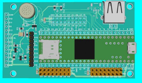
I have a first pass at quick and dirty PCB, that is still same size as ILI9341... Note we can also plug in ILI9488 EBAY verssion...

Still has partial kitchen sink .
screenshot.jpg

Have connections for display to go on back have circuit to dim display looks like need to change pin as current one does not support PWM . On front have Camera connections, have possible add of speaker with simple transistor/diode amp,

Have ability to plug in Adafruit RFM95 like...

Will probably order some. Hopefully not too bad...

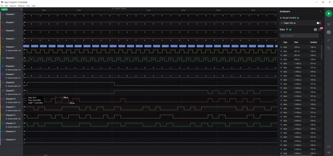
Quick Update. I move my Logic 16 to the setup using CSI... Using the camera pin order which hopefully I have right on the plug area:
screenshot.jpg

So I ran it using the latest Beta Logic setup... Bu this type the 8 data pins were not the first 8 pins on analyzer... Looks like they Basic Parallel analyzer has some issues:
screenshot.jpg
 
Last edited:
@mjs513 - I think I may have found some of our main issues with current sketch ;)

The main sketch has a call: cameraSetResFormat(RGB565, QVGA_320x240);

The actual function: bool cameraSetResFormat(uint8_t res, uint8_t format) {

Helped to change that initial call to: cameraSetResFormat(QVGA_320x240, RGB565);

Also as places were using:
Code:
  FRAME_WIDTH = 320;
  FRAME_HEIGHT = 240;
in many places. I changed the header file to make then extern uint16_t defines.

The main init them to 640 by 480

But after your call I then did:
Code:
//  cameraSetResFormat(RGB565, QVGA_320x240);
  cameraSetResFormat(QVGA_320x240, RGB565);

  // BUGBUG: other places use FRAME_WDITH and FRAME_HEIGHT so lets set them
  FRAME_WIDTH = 320;
  FRAME_HEIGHT = 240;
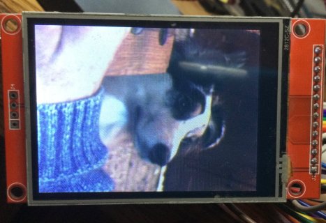
And I am seeint some data on the ILI9341 display :D

Very cool - does the image look like what you are pointing it at. Sorry about the confusion - did that very early in the morning - then to transpose things. Also thought I fixed it so it was defined in the function call for cameraResFormat - have to check.
 
KurtE: It looks like the header near the SD card socket might prevent removal of the SD card. It the T4.1 is elevated on a socket strip, you might be OK, especially if you use a right-angle header.
 
@KurtE

Used your updated sketch and attached a ILI9341 using new jumpers and the new camera (just in case I messed something up the new one). Also put it on my big proto board.

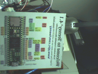
Ran it in 320x240 mode and dumped to the ILI9341 and displayed very nicely, used the T4,1 card as the same. Also dumped to the Arducam windows ap and it worked as well, except image was backwards:
22-53-33.png

Wonder how it would do at movies - guess thats next up.
 

Attachments

  • 22-53-33.bmp
    150.1 KB · Views: 67
@KurtE

As a stress test took the send_tft() and put it into the loop it would continuously send images to the tft. Actually worked pretty good so you could make a Live stream to the ILI9341. Some flicker and pause.

Going to play more later with the camera but have a few things have to do first.
 
@mjs513 - Yep that is along the next line I am/was going to do.

The current one simply displays the frame and waits until it completes. No frame buffer or anything... Was thinking of turn on frame buffer, and when get a frame display it..
Then if the spirit moves us, could try display continuous updates, could even maybe play around with double buffers for both display and camera.
Something like have a pool of 4 buffers (assuming buffers are directly usable for both camera and display), So maybe when the camera finishes one of the frames, it does an ISR that assigns that buffer to the next one the display should pick up and grabs a free buffer and assigns it to camera... Have the TFT code have a DMA chain for two full updates of the screen. When it finishes the last DMA for one screen, it checks for completed frame to substitute in and releases its previous buffer back to pool...

Agian I am sure there are interesting gotchas also not sure if it is worth the try, especially since just doing for the fun of it.
 
Actually wasn't bad the way it is but would be interesting exercise to try. Want to add in a few more options for register controls. Now that it works for the most part should not be too difficult - did something like that when playing around with the OpenMV camera so..... just can't help myself :)

Too many projects :)
 
...could even maybe play around with double buffers for both display and camera.
Something like have a pool of 4 buffers (assuming buffers are directly usable for both camera and display), So maybe when the camera finishes one of the frames, it does an ISR that assigns that buffer to the next one the display should pick up and grabs a free buffer and assigns it to camera...

That is a lot like the SCI demo in the MCU Expresso. I had to download 1.5GB of IDE and other stuff to get the source for the NXP SCI demo for the RT1050, but it was worth it to look over their source code. Their plan is to implement a queue of frame buffers. The SCI filled the buffers and added them to the queue with an interrupt at the end of each frame. during the interrupt handler, the code put the next buffer's address into the DMA address register for the next transfer. The LCD display handler pulled buffers from the queue for display.

I am going to implement a smaller version for my OV7670 library. In my case, I will just have a third frame buffer for screen capture. When a capture is requested, the library will assign the capture frame buffer for the next frame. When that is complete, it will reset to the usual double-buffered alternating frames. That means that you have an unchanging screen capture in a frame buffer that you can process to search for shapes, etc. etc.
 
I updated the CSI_41 sketch so it now supports
  1. setBrightness
  2. setContrast
  3. setLightModes, eg, Auto, Home, Office, Sunny etc
  4. setSE (Special effects) eg, Antique, BW etc - not working correctly, not sure why yet.

Have fun
 

Attachments

  • CSI_41_main.zip
    31.2 KB · Views: 46
@mjs513 and @mborgerson and all:

I just went through and edited the code to use the CSI_REGISTER names instead of using things like x = (1 << 18);...

I found a few ones that were wrong in my earlier PR to imxrt.h which I just issued new one and Paul already pulled in.

Take a look and see what you think.

Note: In one header file I duplicated the ones I put into IMXRT with a #ifndef ... so that once you have updated core, no longer needed.

I also only slightly the mainline function as there was a set of if (ch == 'c') or the like and then a switch statement lower which was not under if (Serial.available()... So merged the two into one switch statement.


FYI - Yes the SD card area is close to where potentially I might plug in an RFM69/95 breakout... So would need to keep low or be able to unplug... But again not sure I will ever populate it.
Ordered from PCBWay so they will probably have ready to ship by Monday by DHL so probably hear sometime next week.
 

Attachments

  • CSI_41_main-201031a.zip
    32 KB · Views: 51
Also I am playing around with a simple videoish command that runs real simple...

Add message: Serial.println("v - Send continuous images to ILI9341");

Just added case to loop: case 'v': do_tft_like_video(); break;

And function that outputs the next frame either 1 or 2 that changes
Code:
void do_tft_like_video() {
  uint32_t fbc1, fbc2;
  uint16_t *pfb;
  uint16_t image_offset_y = (FRAME_HEIGHT - tft.height()) / 2;
  uint16_t image_offset_x = (FRAME_WIDTH - tft.width()) / 2;
  uint32_t tft_image_offset = ((image_offset_y * FRAME_WIDTH) + image_offset_x) * 2;

  while (Serial.read() != -1); // get rid of any excess characters.
  Serial.println("Starting continuous tft displays (like video) enter any key to exit");
  while (!Serial.available()) {
    fbc1 = fb1count;
    fbc2 = fb2count;
    for (;;) {
      if (fbc1 != fb1count) {
        Serial.printf("FB1: %lu\n", fb1count);
        pfb = (uint16_t*)((uint8_t*)(fb1 + tft_image_offset));  // Point to pixels.
        break;
      }
      if (fbc2 != fb2count) {
        Serial.printf("FB2: %lu\n", fb2count);
        pfb = (uint16_t*)((uint8_t*)(fb2 + tft_image_offset));  // Point to pixels.
        break;
      }
    }

    // Lets extract image from center.
    // hard code first pass:
    uint16_t *pimage = image;
    //Serial.printf("Image offsets: X:%u Y: %u bytes: %lu Total: %lu\n", image_offset_x, image_offset_y, tft_image_offset, imagesize);

    uint16_t *pfb_row = pfb;
    for (int row = 0; row < (int)tft.height(); row++) {
      pfb = pfb_row;
      for (int col = 0; col < (int)tft.width(); col++) {
        *pimage = *pfb++;
        // Lets get an idea of data coming in.  How about center 16x16 pixels.
        pimage++;
      }
      pfb_row += FRAME_WIDTH;
    }
    tft.writeRect(0, 0, tft.width(), tft.height(), image);
  }
  while (Serial.read() != -1); // get rid of any excess characters.
  Serial.println("*** Exiting video mode ***");

}

Code:
Starting continuous tft displays (like video) enter any key to exit

FB1: 780
FB2: 779
FB1: 781
FB2: 780
FB1: 782
FB2: 781
FB1: 783
FB2: 782
FB1: 784
Looks like we are completing our screen updates faster than we are receiving frames...

It does give you flashing, probably no way for us to get in sync with when the display is set to best update.
 
Status
Not open for further replies.
Back
Top