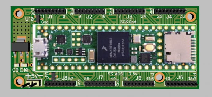
Teensy40 - only 3.3V power supply?

Hello
I am a newby and this could possibly be a dumb question, appologies.
I am transitioning from an Arduino Due based project to using a Teensy40, basically because of the smaller footprint. (But I have to admit it is a very sweet device!)
On the Arduino project I currently use an input voltage of 7.5V that is regulated down to 3.3V on the Due board. I then use this 3.3V from the Due to power a whole heap of other chips for my project. The Due allows up to 800ma draw. I use a 7.5V supply as this is required elsewhere in my project.
With the Teensy40 it looks different. The max input voltage is 5.5V and the max draw on the 3.3V line is 250ma.
My question is:
Can I use one regulator, 7.5 to 3.3V to supply both the Teeny and my other chips? (i.e. no Vin supplied to the Teensy - there will be no USB connection.)
OR
Must I use two regulators 7.5 to ~5V for Teensy Vin AND 7.5V to 3.3V for my chips?

The question boils down to: can the Teensy40 run from only a 3.3V input?

Many thanks for your patience in getting this far. Thanks for any help.

Nigel
 
can the Teensy40 run from only a 3.3V input?

Teensy 4.0 was not designed to be powered this way. It can be made to work, but you should be aware of the startup sequencing requirements (which currently are not yet well documented).

The main issue is Teensy 4.x needs power on its SNVS input before or simultaneously with the other power inputs, except USBx_VBUS. If you apply power to the NVCC_xxx pins or VDD_HIGH_IN or VCC_ADC before SNVS, or if you externally drive any I/O pins while SNVS is off which bleeds power through the ESD protection diodes to the chip's internal power rails, the chip may fail to start up because SNVS wasn't powered first or at least simultaneously.

To be more specific, this means applying power to the VDD_SNVS_IN pin and allowing enough time for the capacitor connected to VDD_SNVS_CAP to charge up. If power gets applied to the other pins before that SNVS capacitor reaches about 1.0 volt, the chip may not start up.

Normally when you apply power to VUSB or VIN, the 3.3V regulator is kept off by a 100K resistor connected to its enable pin. The incoming power does go to USB1_VBUS and USB2_VBUS. The USB VBUS regulator is an exception to the "SNVS first" rule, as it's fully independent of the rest of the chip's startup sequence.

With USB power applied to those 2 pins, the capacitors on VDD_USB_CAP start to charge, reaching about 2.5 volts.

VDD_SNVS_IN starts to get power as VDD_USB_CAP charges up, because it's connected by a BAT54C diode. Keep in mind VDD_SNVS_IN will be "behind" VDD_USB_CAP due to the forward voltage drop of the diode. The diode's forward voltage drop causing effectively a delay is an important point to keep in mind if you power Teensy 4.x in alternate ways where the power rises slowly.

In the normal startup sequence, once VDD_SNVS_CAP is charged, the chip's internal power management and security hardware boots up. Within several milliseconds, it drives PMIC_ON_REQ high. Keep in mind logic high on that pin is about 1.1V at this early stage. The 3.3V regulator we use on Teensy 4.x is rated to work with 1V enable. Regulators needing a higher logic voltage won't work.

As the 3.3V power come up, the DCDC buck converter remains off due to a 100K resistor connected to DCDC_PSWITCH. The VDD_HIGH_CAP and NVCC_PLL capacitors start to charge up.

The MKL02 chip boots up and configures its brown-out detection for approx 2.9V. It then waits several milliseconds for the 3.3V power to be stable and then drives DCDC_PSWITCH high, which causes the buck converter to start creating the 1.15V power the main CPU needs to start. NXP's documentation gives a wrong impression that DCDC_PSWITCH may be level sensitive. It is not. A rising edge after 3.3V is stable is required to make the DCDC buck convert start.

The MKL02 also drives POR_B high after another short delay, which lets the main IMXRT chip boot.


If you try to power Teensy 4.0 with only 3.3V power, you'll be skipping the first half of this power up sequence. Remember, the voltage at VDD_SNVS_IN is slightly "behind" due to the BAT54C forward voltage drop. If your 3.3V power rises very quickly to at least 1.5V, you may be able to get power to VDD_SNVS_IN and VDD_SNVS_CAP fast enough for the chip to start up. But if your 3.3V power is created by a power supply with "soft start" or a linear power supply with large capacitors, it will probably rise too slowly.

There are a couple possible workarounds. As you can see on the Teensy 4.x schematic, the cathode of all those diodes which connect to VDD_SNVS_IN come to a test point. If you short that test point to 3.3V power, then VDD_SNVS_IN will no longer be "behind" or delayed from the 3.3V rise.

The other alternative is to arrange for VBAT to have power before you apply the main 3.3V power. Maybe a resistor and zener diode or LED to create a low power 2-3V input to VBAT would be used from your unregulated power. Only a fraction of a milliamp is needed.
 
Hi Paul
Many thanks for your quick and comprehensive reply. There is much here to digest and it will take me some time to do it, but a quick read through indicates that it would be easier/safer to have two regulators & for the cost of a few coppers.
Wow, it's good to know that there is such good back-up around. Thanks again.
Nigel
 
I know this is a slightly old thread but i wanted to know Paul if i was to add a coin battery to Vbat would that do the trick. i had already designed a board with the Teensy 4.1 in mind yet i was unaware of the 3.3 v difficulties at the time. i would hate to have to redesign my board. also will this just be needed for the start up sequences yet run fine when disconnected after start up.
Please advise,
Marathonman
 
Thanks Paul and Yes i am aware of the link and info. it is possible in my situation that i can change the voltage reg to from 3.3 v to 5 v to power V in and use a shift register that can interface both 5 and 3.3 v systems. the Toshiba shift register 74VHC595FT i think will allow me to do this which will be powered with 5 v and the input from Teensy 4.1 SPI output will of course be 3.3v. the outputs of the shift registers will then go to high side drivers.
this startup sequence with the NXP chips is a real pain in the back side and threw my hole board design in left field.

thank you for your response as i know your time is very short.
Marathonman
 
The possibly more easily sourced 74HCT family (5V supply only) will handle 3.3V inputs too,
but the 74VHC family can be powered from either 3.3 or 5V and still work with "TTL level" inputs.

74HC itself is not spec'd to handle 3.3V inputs when powered from 5V supply.
 
The HCT series is 4.5 V to 5.5 V thus the reason i did not choose it in the first place. the easily sourced is not a problem with the 74VHC595FT as Mouser has over 5 thousand of them. the spec sheet says 0 to 5.5 volts input unless i am missing something.

So if i change my board design to connect to the V in pin with 5 volts and leave the rest of the board and shift registers i should be fine. the Fan high side drivers are rated for high input at 2.5 volts so i am good there. i do think i will cut the usb power connection as i see me reprogramming in place in the furture as i add features like sensor readout, display connection as well as the electronic high side switching i already have in place.
 
I just meant the HCT family is easier to source than the VHC due to the greater number of manufacturers
and higher volume of sales for the family traditionally used for 3.3 -> 5V level shifting. VHC is fairly new
I think, perhaps only single-sourced even.

BTW I think you want VHCT family if the input can be 3.3V and the supply might be 5V.
 
I do agree and also agree with the VHCT part . was reviewing yesterday and the high input is at 2 volts. the VHC part is higher at 3.85v so yes i will go with the VHCT. having the larger overhead will be nice even though the SPI is being clocked at 1 Mhz then the buffer shifted at 300 us it is still good to have overhead. good part about is i can have Schmit trigger inputs which i like for possible noise.
4.1 Shift Reg Timing.PNG
Teensy 4.1 8 Shift Registers.PNG

i am planing on mounting a 4.1 on a very small board for just enough room for the 4.1 with 1.25 mm connectors on each side with voltage reg on end. as you see it is not much bigger then the 4.1.
Thanks, good input Mark
Regards,
Marathonman
 
Last edited:
There are a couple possible workarounds. As you can see on the Teensy 4.x schematic, the cathode of all those diodes which connect to VDD_SNVS_IN come to a test point. If you short that test point to 3.3V power, then VDD_SNVS_IN will no longer be "behind" or delayed from the 3.3V rise.

I can't find the test point on the board. Can you point me to the right direction.

Thanks
 
By the way the VHCT shift register solved all my problems being fed 5 volt and the Teensy 3.3 volt. the input on the VHCT goes high at 2 volt and can handle the voltage difference between it and the Teensy. i have a youtube video of it hitting it out of the ball park. plus the program i have had help with is so perfect for what i need with make before break and ends on 5 times longer for my inductive roll off. the 4.1 froze up but the 4.0 works outstanding.
Thanks Paul for a good product and vision.
Regard,
Marathonman
 
Teensy 3.2 to 4.0 transition.

My solution (probably sub optimal but safe) is to power the teensy 4.0 from the existing regulator (5 volt in my case) and add a 3.3 volt regulator to power all peripherals. My peripheral load on the 3.3V was getting up to 200mA when I subbed in 3.3 volt RS-485 and RS-232 chips. Decoupling caps took the start up current above that. In addition I have a teensy controlled high side switch to reset the peripherals (mainly the A/D) if they don't start up right. This is very useful when switching from USB to local power during debug.


Hello
I am a newby and this could possibly be a dumb question, appologies.
I am transitioning from an Arduino Due based project to using a Teensy40, basically because of the smaller footprint. (But I have to admit it is a very sweet device!)
On the Arduino project I currently use an input voltage of 7.5V that is regulated down to 3.3V on the Due board. I then use this 3.3V from the Due to power a whole heap of other chips for my project. The Due allows up to 800ma draw. I use a 7.5V supply as this is required elsewhere in my project.
With the Teensy40 it looks different. The max input voltage is 5.5V and the max draw on the 3.3V line is 250ma.
My question is:
Can I use one regulator, 7.5 to 3.3V to supply both the Teeny and my other chips? (i.e. no Vin supplied to the Teensy - there will be no USB connection.)
OR
Must I use two regulators 7.5 to ~5V for Teensy Vin AND 7.5V to 3.3V for my chips?

The question boils down to: can the Teensy40 run from only a 3.3V input?

Many thanks for your patience in getting this far. Thanks for any help.

Nigel
 
Back
Top