As we know, The T4 SPI peripheral can only toggle one CS pin, and the CS pin selection is no longer in the transmit data FIFO. Being able to control multiple CS pins from the transmit FIFO was useful for driving SPI displays because the displays often have a Data/Command pin that needs to be driven in addition to the CS pin, and having the CS pin control in the transmit FIFO allowed a mix of commands and data to be sent to the SPI peripheral via DMA.
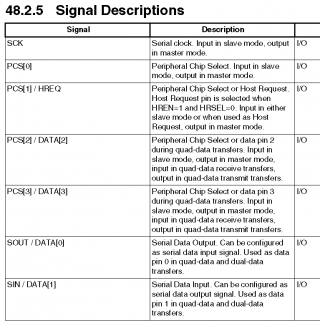
What T4's SPI gained was support for 2-bit and 4-bit half duplex SPI. By crafting the data correctly, it is possible make the normal MOSI data come out of one data line and the DC value come out of another, once again allowing DMA to be used to send a mix of commands and data. See the reference manual for the pin mappings in 2/4 bit mode:
Whether this will work for your display depends on the timing requirement of the display. If the display requires the DC value to be valid before the clock line goes down for the first time, then it won't work. If the display only requires the DC value to be valid towards the end of the transfer, then it will likely work. I tried this on a Noritake GU128X64-800B VFD and it worked great. (code)
Caveats:
1. The 2-bit and 4-bit SPI modes are half duplex, so you can't transmit and receive at the same time. You need to switch back to 1-bit mode to do that.
2. The MISO line is used as DATA[1] when running in 2 or 4 bit mode, and it is an output when transmitting. If you have the MISO line hooked up, then you need to put a resistor between the teensy and the display so you don't connect 2 outputs together.
Let's look at the timing requirement of a few SPI display controllers.
GU128X64-800B
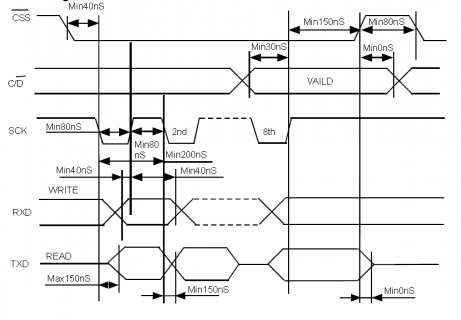
The display only requires the D/C pin to be valid at the end of the transfer.. This will work.
ILI9341
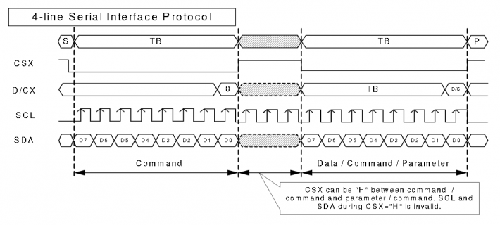
Again, the D/C is read at the same time as the last bit. This will work.
HX8357

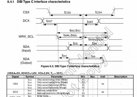
The D/C is read at the same time as the first bit and it must show up no later than the first falling SCK edge. The timing is going to be tight. You may be able to make it work by playing with the slew rate and drive strength on the pins for SCK and D/C to make D/C a bit faster than SCK.
SSD1306
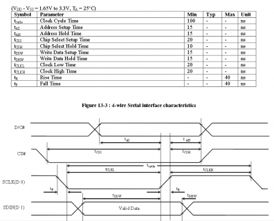
The D/C valid period is defined relative to the rising clock edge and the timing requirement is the same as for the data. This will work.
I hope this information is useful.
What T4's SPI gained was support for 2-bit and 4-bit half duplex SPI. By crafting the data correctly, it is possible make the normal MOSI data come out of one data line and the DC value come out of another, once again allowing DMA to be used to send a mix of commands and data. See the reference manual for the pin mappings in 2/4 bit mode:

Whether this will work for your display depends on the timing requirement of the display. If the display requires the DC value to be valid before the clock line goes down for the first time, then it won't work. If the display only requires the DC value to be valid towards the end of the transfer, then it will likely work. I tried this on a Noritake GU128X64-800B VFD and it worked great. (code)
Caveats:
1. The 2-bit and 4-bit SPI modes are half duplex, so you can't transmit and receive at the same time. You need to switch back to 1-bit mode to do that.
2. The MISO line is used as DATA[1] when running in 2 or 4 bit mode, and it is an output when transmitting. If you have the MISO line hooked up, then you need to put a resistor between the teensy and the display so you don't connect 2 outputs together.
Let's look at the timing requirement of a few SPI display controllers.
GU128X64-800B

The display only requires the D/C pin to be valid at the end of the transfer.. This will work.
ILI9341

Again, the D/C is read at the same time as the last bit. This will work.
HX8357


The D/C is read at the same time as the first bit and it must show up no later than the first falling SCK edge. The timing is going to be tight. You may be able to make it work by playing with the slew rate and drive strength on the pins for SCK and D/C to make D/C a bit faster than SCK.
SSD1306

The D/C valid period is defined relative to the rising clock edge and the timing requirement is the same as for the data. This will work.
I hope this information is useful.

