Routing pll5 to an output pin on teensy 4.1

hobi

Member
Hi all,
I read with great attention the vga code using flexio 1/2 and dma to have a functional 8 bit vga using teensy 4.1. I try to build a tft interface for a buffer less contrôler. I need pixel clock for that to go on an output pin. I looked/crawled in the super long reference manual and I could not identify how to get pll5 on an output pin. For sure pll5 can be fed to multiple blocks but I did not saw an output pin possibility so far… any help appreciated!

Thanks in advance
 
Maybe you can simply use one of the i2s and its mclk pin. All the rest of i2s would just be dummy and all other i2s pins not enabled / assigned to i2s.
I used this for an fm transmitter.
 
Last edited:
Hmm that should work. Pll5 routed to the SAI clocks, and basically discarding any i2s related code after clock setup. Thank you - will give a try!
 
It DOES work :)

For those of us less technically inclined, how would we do this? Specifically, I'm routing all the VGA signals (from VGA_t4 by J-M Harvengt) to an FPGA to create an HDMI output. However, I need both a DE and Pixel Clock signal (from the Teensy 4.1 to the FPGA) to make it work.

Could anyone suggest some Arduino IDE code to make this work (in a sketch that uses the VGA_t4 library)?
 
Two posts before I posted a link to some code.

Frank,

Thanks for the fast reply! :)

Yes, I did see that. But, like I implied, my "thing" is really FPGAs and hardware, not so much MCUs and embedded code - I'm just in a position where, sometimes, it is helpful to use them (particularly the Teensy). Stated differently, I'm kind of a "dummy" when it comes to this stuff :p

But seriously, if you could maybe elaborate further, and spell it out for this mcu "dummy", it would be greatly appreciated!

Lol, thanks again!

Jon
 
:cool: Much appreciated!

Note, it uses this padconfig: #define PADCONFIG ((0 << 0) | (1 << 3) | (1 << 6)) //Pg 622 Reference Manual
Which sets "slow" slew rate etc. I had to use slow settings to "round" the edges of the square wave as much as possible - because it's used analog"ish" and is directly connected to the antenna.
You want "fast".

So, for fast, I see, according to your notes:

#define PADCONFIG ((1 << 0) | (1 << 3) | (1 << 6))

The other settings, regarding the CCM clock divider register:

CCM_CS1CDR_SAI1_CLK_PRED(carrier.i2s_clk_pred - 1)
CCM_CS1CDR_SAI1_CLK_PODF(carrier.i2s_clk_podf - 1);

Any idea what the proper settings are (Divider for sai1 clock pred and Divider for sai1 clock podf)?

It's probably more convenient to just share the link to the code I'm modding:
https://github.com/Jean-MarcHarvengt/VGA_t4/blob/master/VGA_t4.cpp

I have to stick this all in there - somewhere :D

Jon

PS I normally wouldn't invest so much time into this, but I think it will help a lot of other people with the same dilemma (who find this post), and there are probably many, many others who might find this useful.

PPS These are the frequencies (probably helpful):
#define frame_freq 60.0 // Hz
#define line_freq 31.46875 // KHz
#define pix_freq (line_freq*800) // KHz (25.175 MHz)
 
Note, it uses this padconfig: #define PADCONFIG ((0 << 0) | (1 << 3) | (1 << 6)) //Pg 622 Reference Manual
Which sets "slow" slew rate etc. I had to use slow settings to "round" the edges of the square wave as much as possible - because it's used analog"ish" and is directly connected to the antenna.
You want "fast".

Wait... could it be as simple as this?

#define PADCONFIG ((1 << 0) | (1 << 3) | (1 << 6))

// Select MCLK
IOMUXC_GPR_GPR1 = (IOMUXC_GPR_GPR1 & ~(IOMUXC_GPR_GPR1_SAI1_MCLK1_SEL_MASK))
| (IOMUXC_GPR_GPR1_SAI1_MCLK_DIR | IOMUXC_GPR_GPR1_SAI1_MCLK1_SEL(0));
I2S1_TMR = 0;
I2S1_TCR2 = I2S_TCR2_MSEL(1);
CORE_PIN23_CONFIG = 3;
CORE_PIN23_PADCONFIG = PADCONFIG;
 
Nope - that doesn't work. The pixel clock is in the video pll - that's what has to be routed out; but I don't have the background to do it.
 
That is SAI1, then.

Good luck :)

Haven't been able to get it to work. First, there was a nascent, experimental audio driver tucked away at the end of the VGA file, which happened to use SAI1 and pin 23; so, that was why the first attempt had to fail.

The pixel clock (25.175 MHz) is routed through the video pll 5. So, do I need to use a new clock, or is there a way to route that specific clock instance to, for example, SAI3 and Pin 30?

Thanks, @Frank B. I'm hanging on your every word :D

Jon
 
Nope - that doesn't work. The pixel clock is in the video pll - that's what has to be routed out; but I don't have the background to do it.

You need to set all registers:
Code:
        CCM_CCGR5 |= CCM_CCGR5_SAI1(CCM_CCGR_ON);
        CCM_CSCMR1 = (CCM_CSCMR1 & ~(CCM_CSCMR1_SAI1_CLK_SEL_MASK))
                     | CCM_CSCMR1_SAI1_CLK_SEL(1); // &0x03 // (0,1,2): PLL3PFD0, PLL5, PLL4
        CCM_CS1CDR = (CCM_CS1CDR & ~(CCM_CS1CDR_SAI1_CLK_PRED_MASK | CCM_CS1CDR_SAI1_CLK_PODF_MASK))
                     | CCM_CS1CDR_SAI1_CLK_PRED(carrier.i2s_clk_pred - 1) // &0x07
                     | CCM_CS1CDR_SAI1_CLK_PODF(carrier.i2s_clk_podf - 1); // &0x3f

        // Select MCLK
        IOMUXC_GPR_GPR1 = (IOMUXC_GPR_GPR1 & ~(IOMUXC_GPR_GPR1_SAI1_MCLK1_SEL_MASK))
                          | (IOMUXC_GPR_GPR1_SAI1_MCLK_DIR | IOMUXC_GPR_GPR1_SAI1_MCLK1_SEL(0));
        I2S1_TMR = 0;
        I2S1_TCR2 = I2S_TCR2_MSEL(1);
        CORE_PIN23_CONFIG = 3;
        CORE_PIN23_PADCONFIG = PADCONFIG;
You also (additional) have to enable and set PLL5..
Which frequency do you need?
 
That's funny! We must have posted at approximately the same exact time! Spooky! :p

25.175 MHz

Oh, as an aside - do I need to modify the VGA library itself with this code, or can I just put it in the sketch?
 
Last edited:
Exactly 25175000Hz?
Maybe I find some time on saturday to post code for all needed values/registers .

VGALib: I don't know. Maybe it needs some other changes, too.
I fear you have to figure that yourself :)

p.s. yes, Spooky :)
p.s.s You know there are 15€ VGA->HDMI converters? I have one - works good.
 
Exactly 25175000Hz?
Maybe I find some time on saturday to post code for all needed values/registers .

VGALib: I don't know. Maybe it needs some other changes, too.
I fear you have to figure that yourself :)

Lol, shouldn't be a problem - going over all this with you, I'm kind of starting to get the hang of it. You're a good teacher! Jon

I should say that as we've done this, step by step, I've been looking up the registers you've pointed me to, amongst the other things, to really understand this for myself. Having to ask for help bruises my ego :cool:
 
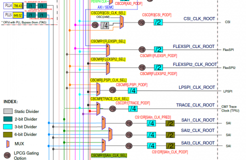
The clock diagram from the ref manual shows (almost) all you need to know:
View attachment 26929
(Yes there is a green line missing ;-)

Missing are only some details about PLL- and SAI Setup.

I don't know anything about FPGA. Some years ago I played a little bit with it.. and the code..... but.. it never found it's way to a FPGA...
 
The clock diagram from the ref manual shows (almost) all you need to know:
View attachment 26929

Missing are only some details about PLL- and SAI Setup.

I don't know anything about FPGA. Some years ago I played a little bit with it.. and the code..... but.. it never found the it's way to a FPGA...

I can't open the link - it says: "Invalid Attachment specified. If you followed a valid link, please notify the administrator"

Without a guide, this documentation is impenetrable. Denser than Microchip PIC documentation! (Yeah, I've tried my hand at that, too). Bleh!
 
Next try:
2021-12-16 16_48_17-IMXRT1060RM REV2.pdf - Adobe Acrobat Reader DC (32-bit).png

If it does not work: you can find it on page 1016 in the ref manual rev 2.
 
Back
Top