Hey all! 
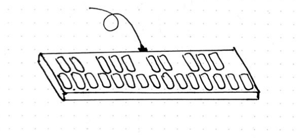
I've had this idea for a while to try to make a 25-key MIDI keyboard based on Inductive Sensors. The rough idea is to lay out a coil per key to make an inductor, and hook that up to an Inductance-To-Digital converter. Then just read those values into a Teensy LC and spit some MIDI out The cool thing would then be to map out in software how strong you're pressing the key to vary the MIDI notes sent out the device. A good example would be to hook it up to the volume so you have decent dynamic range when playing and can go as quiet/loud by just pressing soft/hard. Here you have the worst drawing you'll ever see:
This is really my first "real" PCB and project like this. I've made PCBs for the Teensy before but pretty much just as "project specific breakout boards" that didn't involve much or any electronics. So please let me know if something looks off or wrong. It's very likely that I missed obvious things.
How it's supposed to work
The setup would have the main PCB (with the teensy and the coils in it) on the bottom, then a spacer PCB in the middle that has no copper, just holes where each of the keys would be. On top of that there will be an aluminium sheet. The idea is that when you press the aluminium that is floating on top of a coil (because of the hole), the metal should bend very slightly, which is enough for the coil and the sensor to pick it up and convert it to a digital signal, like this:
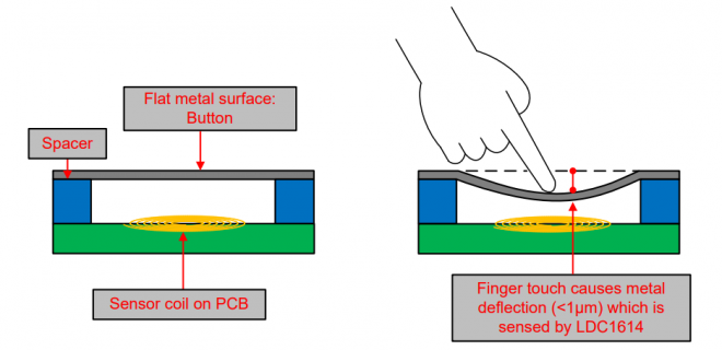
For a way better explanation check out this document from Texas Instruments (https://www.ti.com/lit/an/snoa951/snoa951.pdf). In Figure 10 you can see a very similar setup to what I'm trying to achieve.
A general explanation of Inductive Sensing also in this video: https://www.youtube.com/watch?v=cnNDUyTttrM
Schematic
I'm attaching the current schematic I made in KiCad to this post. The gist of it is a USB-A connector that goes into an ESD protection chip, then the +5V goes into a regulator to get +3.3V to power up the LDC Converters (Inductance-To-Digital converters) and their oscillators. Each of the LDC chips connects to some of the coils, trying to keep the distance between the chips and the coils as short as possible.
There's the Teensy LC, that I was going to just power by connecting the +5V from the USB cable to VUSB. Also obviously connected to the USB Data lines.
And from the Teensy, one set of the SCL/SDA pins will go to a I2C multiplexer that then will connect to the 8 LDC sensors spread on the board.
Please see the attached View attachment schematic.pdf file.
Layout
I laid out the coils on the PCB using KiCad with some custom code I wrote to generate the coils (since I'd have to do them by hand otherwise with small segments). Here you can see my rough sketch of how I think I'd put everything together.
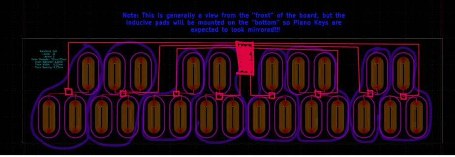
The PCB is 40x10cm. In the center I'd like to mount the Teensy, I2C multiplexer, USB-A female terminal and the Voltage Regulator, hopefully making everything fit.
Then from the multiplexer, the red lines show where I was thinking I could route the traces to get to the 8 LDC chips, and then finally each chip has a trace to the inductance coils. These are recommended to keep as short as possible so that's why I'm trying to move the LDC chips close to the cluster of coils they'll manage.
Questions/Worries
As I mentioned above, this is my first time setting up a design like this, so anything that looks off please let me know. I'll also happily take any advice on pretty much anything related to this Some more specific questions I had were:
Thank you all for your time and help! And sorry if this is a longer post than normal.
I've found this forum incredibly helpful before and I hope to learn more and become one of the people helping out here in the future
Cheers!
I've had this idea for a while to try to make a 25-key MIDI keyboard based on Inductive Sensors. The rough idea is to lay out a coil per key to make an inductor, and hook that up to an Inductance-To-Digital converter. Then just read those values into a Teensy LC and spit some MIDI out

This is really my first "real" PCB and project like this. I've made PCBs for the Teensy before but pretty much just as "project specific breakout boards" that didn't involve much or any electronics. So please let me know if something looks off or wrong. It's very likely that I missed obvious things.
How it's supposed to work
The setup would have the main PCB (with the teensy and the coils in it) on the bottom, then a spacer PCB in the middle that has no copper, just holes where each of the keys would be. On top of that there will be an aluminium sheet. The idea is that when you press the aluminium that is floating on top of a coil (because of the hole), the metal should bend very slightly, which is enough for the coil and the sensor to pick it up and convert it to a digital signal, like this:

For a way better explanation check out this document from Texas Instruments (https://www.ti.com/lit/an/snoa951/snoa951.pdf). In Figure 10 you can see a very similar setup to what I'm trying to achieve.
A general explanation of Inductive Sensing also in this video: https://www.youtube.com/watch?v=cnNDUyTttrM
Schematic
I'm attaching the current schematic I made in KiCad to this post. The gist of it is a USB-A connector that goes into an ESD protection chip, then the +5V goes into a regulator to get +3.3V to power up the LDC Converters (Inductance-To-Digital converters) and their oscillators. Each of the LDC chips connects to some of the coils, trying to keep the distance between the chips and the coils as short as possible.
There's the Teensy LC, that I was going to just power by connecting the +5V from the USB cable to VUSB. Also obviously connected to the USB Data lines.
And from the Teensy, one set of the SCL/SDA pins will go to a I2C multiplexer that then will connect to the 8 LDC sensors spread on the board.
Please see the attached View attachment schematic.pdf file.
Layout
I laid out the coils on the PCB using KiCad with some custom code I wrote to generate the coils (since I'd have to do them by hand otherwise with small segments). Here you can see my rough sketch of how I think I'd put everything together.

The PCB is 40x10cm. In the center I'd like to mount the Teensy, I2C multiplexer, USB-A female terminal and the Voltage Regulator, hopefully making everything fit.
Then from the multiplexer, the red lines show where I was thinking I could route the traces to get to the 8 LDC chips, and then finally each chip has a trace to the inductance coils. These are recommended to keep as short as possible so that's why I'm trying to move the LDC chips close to the cluster of coils they'll manage.
Questions/Worries
As I mentioned above, this is my first time setting up a design like this, so anything that looks off please let me know. I'll also happily take any advice on pretty much anything related to this
- Can I power the Teensy LC with the +5V from USB like I'm doing in the schematic, pretty much directly out of the terminal, into the ESD protection chip, then into VUSB? I struggled to figure out if the way I'm trying to do the power delivery made sense.
- Would the "long" traces from the multiplexer to the LDC chips be a problem? I checked some pages to calculate the pull-up resistor values and it seemed to look fine but I'm not sure.
- Because of the placement of the keyboard keys, I'm having to do some wiring in the middle of the inductance coils, do you think this could be a problem?
- I tried to do all the research I could on the values for pull-up resistors, bypass capacitors, etc. But I'm not 100% sure everything is correctly put together.
- For pull-up resistors, where would you physically put them? Close to the output of the multiplexer or close to the LDC chip?
- I've seen people mention to put a resistor on the output of the oscillators to dampen ringing, is this necessary?
Thank you all for your time and help! And sorry if this is a longer post than normal.
I've found this forum incredibly helpful before and I hope to learn more and become one of the people helping out here in the future
Cheers!

