Kuba0040
Well-known member
Hello!
I want to connect my Teensy 4.0 board up to some older chips. I want the teensy to be able to communicate with them. Now these chips, being you know… old. Want their digital signals to be held high or low for let’s say… a minimum of 250ns. That would constitute a clock of 4MHz.
Now, the digitalWriteFast function is waaaay to fast for these chips, now I could just add nops in between the digitalWriteFast commands, but that’s just wasting CPU time, and I just have a feeling that on ARM, there must be a better way to do this than just brainless bit-banging with the CPU.
I’ve seen in the past the maker Bitluni use on the ESP32 some mysterious I2S pipeline with FIFO buffers to drive a VGA display without the CPU’s involvement! Is there a way to do something similar where I could setup some hardware in the Teensy to communicate with this old chip, and it would keep the signals at correct clocks and bit bang the data out by itself? And the teensy’s CPU, would when it wants to communicate with the chip, just send to that special hardware module a message like: “Hey! Send out this binary string:”. And the hardware would do the bit banging itself.
So, basically, I am asking does a module like this exist in the Teensy 4.0? If so what’s its name so I can learn how to use it.
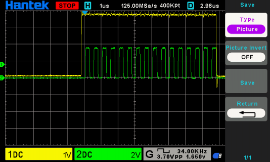
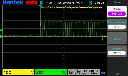
If it helps, the chip I am trying to communicate with (YM3014) only has 3 wires, it works like a shift register so pull LOAD low, then send bits one after another pulsing the CLOCK line high every time you do so, then halfway in pull LOAD high, and then once you have sent all the bits just pull LOAD low. I would like to just be able to give the hardware module in the teensy the bits to send, and it would do all the communication work all by itself, so the CPU can do other things.


