Kuba0040
Well-known member
Hello,
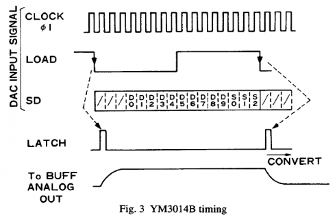
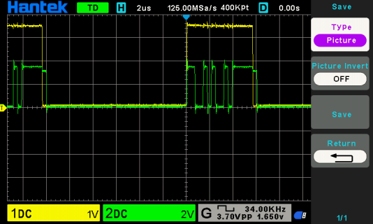
I would like to use the I2S functionality that the Teensy 4.0 has to communicate with a DAC chip. To do this I've dug up the output_i2s.h file written by Paul Stoffregen. Along with his accompanying forum post I was able to roughly figure out what each part does, and with some slight tweaks managed to get the clocks running and send out data. Slight issue...
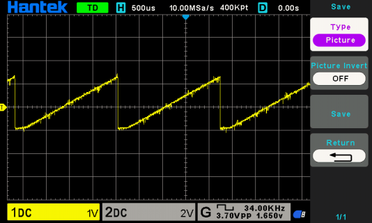
The way I am sending data right now is just by shoving it into the I2S1_TDR0 register. This presents some problems. First of all, I have no control over which channel does the data end up in. Also, as you can see in this simple loop (void loop, second code field), if the delayMicroseconds function goes above 5 the data flow stops completely. I know that originally Paul envisioned the DMA to send out audio data in readymade chunks of some set number of samples, however I'd like a more direct approach where the I2S just spits out a sample at the correct channel until a new one has been set. Is this even possible? If so, how do I do all the things mentioned here and how do I do them properly?
Thank You.
Here is Paul's code I commented with the things I figured out, as well as made some minor modifications to fit the I2S data format I want:
And here is the rough way I'm sending data right now, as I said, just shoving it into the I2S1_TDR0 register
I would like to use the I2S functionality that the Teensy 4.0 has to communicate with a DAC chip. To do this I've dug up the output_i2s.h file written by Paul Stoffregen. Along with his accompanying forum post I was able to roughly figure out what each part does, and with some slight tweaks managed to get the clocks running and send out data. Slight issue...
The way I am sending data right now is just by shoving it into the I2S1_TDR0 register. This presents some problems. First of all, I have no control over which channel does the data end up in. Also, as you can see in this simple loop (void loop, second code field), if the delayMicroseconds function goes above 5 the data flow stops completely. I know that originally Paul envisioned the DMA to send out audio data in readymade chunks of some set number of samples, however I'd like a more direct approach where the I2S just spits out a sample at the correct channel until a new one has been set. Is this even possible? If so, how do I do all the things mentioned here and how do I do them properly?
Thank You.
Here is Paul's code I commented with the things I figured out, as well as made some minor modifications to fit the I2S data format I want:
Code:
FLASHMEM void set_audioClock(int nfact, int32_t nmult, uint32_t ndiv) // sets PLL4
{
  CCM_ANALOG_PLL_AUDIO = CCM_ANALOG_PLL_AUDIO_BYPASS | CCM_ANALOG_PLL_AUDIO_ENABLE
           | CCM_ANALOG_PLL_AUDIO_POST_DIV_SELECT(2) // 2: 1/4; 1: 1/2; 0: 1/1
           | CCM_ANALOG_PLL_AUDIO_DIV_SELECT(nfact);

  CCM_ANALOG_PLL_AUDIO_NUM   = nmult & CCM_ANALOG_PLL_AUDIO_NUM_MASK;
  CCM_ANALOG_PLL_AUDIO_DENOM = ndiv & CCM_ANALOG_PLL_AUDIO_DENOM_MASK;

  CCM_ANALOG_PLL_AUDIO &= ~CCM_ANALOG_PLL_AUDIO_POWERDOWN;//Switch on PLL
  while (!(CCM_ANALOG_PLL_AUDIO & CCM_ANALOG_PLL_AUDIO_LOCK)) {}; //Wait for pll-lock

  const int div_post_pll = 1; // other values: 2,4
  CCM_ANALOG_MISC2 &= ~(CCM_ANALOG_MISC2_DIV_MSB | CCM_ANALOG_MISC2_DIV_LSB);
  if(div_post_pll>1) CCM_ANALOG_MISC2 |= CCM_ANALOG_MISC2_DIV_LSB;
  if(div_post_pll>3) CCM_ANALOG_MISC2 |= CCM_ANALOG_MISC2_DIV_MSB;

  CCM_ANALOG_PLL_AUDIO &= ~CCM_ANALOG_PLL_AUDIO_BYPASS;//Disable Bypass
}


// This function sets all the necessary PLL and I2S flags necessary for running
FLASHMEM void config_i2s(int fs) /*The argument here is the sample rate*/
{
  /*CLOCK GENERATION*/
  CCM_CCGR5 |= CCM_CCGR5_SAI1(CCM_CCGR_ON);

  //PLL:
  // PLL between 27*24 = 648MHz und 54*24=1296MHz
  int n1 = 4; //SAI prescaler 4 => (n1*n2) = multiple of 4
  int n2 = 1 + (24000000 * 27) / (fs * 256 * n1);

  double C = ((double)fs * 256 * n1 * n2) / 24000000;
  int c0 = C;
  int c2 = 10000;
  int c1 = C * c2 - (c0 * c2);
  set_audioClock(c0, c1, c2);

  // clear SAI1_CLK register locations
  CCM_CSCMR1 = (CCM_CSCMR1 & ~(CCM_CSCMR1_SAI1_CLK_SEL_MASK))
       | CCM_CSCMR1_SAI1_CLK_SEL(2); // &0x03 // (0,1,2): PLL3PFD0, PLL5, PLL4
  CCM_CS1CDR = (CCM_CS1CDR & ~(CCM_CS1CDR_SAI1_CLK_PRED_MASK | CCM_CS1CDR_SAI1_CLK_PODF_MASK))
       | CCM_CS1CDR_SAI1_CLK_PRED(n1-1) // &0x07
       | CCM_CS1CDR_SAI1_CLK_PODF(n2-1); // &0x3f

  // Select MCLK
  IOMUXC_GPR_GPR1 = (IOMUXC_GPR_GPR1
    & ~(IOMUXC_GPR_GPR1_SAI1_MCLK1_SEL_MASK))
    | (IOMUXC_GPR_GPR1_SAI1_MCLK_DIR | IOMUXC_GPR_GPR1_SAI1_MCLK1_SEL(0));

  /* CONFIGURE OUTPUT PINS
   *  We need to use the RX module as it's pins are easily accesible
   *  the TX module has it's pins on the bottom of the Teensy PCB
  */
  CORE_PIN20_CONFIG = 3;  //1:RX_SYNC  (LRCLK)
  CORE_PIN21_CONFIG = 3;  //1:RX_BCLK
  CORE_PIN7_CONFIG = 3;   //TX DATA OUT

  /*DATA TRANSMISSION
   * The TX module is synchronized to the RX module.
   * The RX module generates the clocks as
   * it's pins are in a normal spot unlike the TX module
  */


  /* DEFINITIONS:
   *  Frame Sync - L/R signal
   */


  /*TRANSMIT MODULE*/
  bool tsync = 1; //1 -> Synchronus operation 0-> Asynchronus

  I2S1_TMR = 0; //I2S pin masking register

  //I2S1_TCSR = (1<<25); //Reset

  I2S1_TCR1 = I2S_TCR1_RFW(1); //FIFO watermark

  I2S1_TCR2 = I2S_TCR2_SYNC(tsync) | I2S_TCR2_BCP // sync=0; tx is async;
        | (I2S_TCR2_BCD | I2S_TCR2_DIV((1)) | I2S_TCR2_MSEL(1));
  /*
   * SYNC - Mode of operation. 0 for Asynchronous where the TX module generates it's own clocks, or 1 for Synchronus, where it synchronizes it's clocks do the RX module.
   * BCP - Bit Clock Polarity. Are we sampling on the FALLING edge (0), or RISING edge (1)?
   * BCD - Bit Clock Direction (when set to 1, like it is here the MASTER generates the bit clock?)
   * DIV - Bit Clock Divide (Divides the Master Clock into the bit clock, aka the one we transmit)
   * MSEL - MCLK Select, selects which MCLK (Master Clock) source for the TX module.
   */

  I2S1_TCR3 = I2S_TCR3_TCE;
  /*
   * TCE - Transmit Channel Enable
   * This enables the individual I2S transmit channels,
   * The teensy has 4 transmit channels so TCE is 4 bits wide
   */


  I2S1_TCR4 = I2S_TCR4_FRSZ((2-1)) | I2S_TCR4_SYWD((16-1)) | I2S_TCR4_MF
        | I2S_TCR4_FSD | I2S_TCR4_FSP;
  /*
   * FRSZ - Frame size, how many words of data are we transmiting?
   * SYWD - Sync Witdh, configures how many bit clocks-1 does one frame consist of?
   * MF - MSB First, configures if MSB or LSB is sent out first. 0 -> LSB. 1 (like here) -> MSB.
   * FSE - Frame Sync (L/R), does it start on the first bit withn a frame(0), or the one before it(1)?
   * FSP - Frame Sync Polarity, is the Frame sync active HIGH? (0) or active low? (1)
   */

  I2S1_TCR5 = I2S_TCR5_WNW((16-1)) | I2S_TCR5_W0W((16-1)) | I2S_TCR5_FBT((16-1));
  /*
   * WNW - Word Width, configures how wide in bits-1, each word is.
   * W0W - Word 0 Width, configures how many bits-1 are in the very first word the I2S sends.
   * FBT - First Bit Shifted
   * Which bit should be sent out first? If we confiured the TX module for MSB first, this value should be
   * greater than or equal to the Word With, and will decrement as we send out the bits. For LSB,
   * it should be smaller or equal to the word with, and will increment up.
   */


  /*RECIEVE MODULE*/
  bool rsync = 0; //1 -> Synchronus operation 0-> Asynchronus

  I2S1_RMR = 0;
  //I2S1_RCSR = (1<<25); //Reset

  I2S1_RCR1 = I2S_RCR1_RFW(1);  //FIFO watermark

  I2S1_RCR2 = I2S_RCR2_SYNC(rsync) | I2S_RCR2_BCP  // sync=0; rx is async;
        | (I2S_RCR2_BCD | I2S_RCR2_DIV((1)) | I2S_RCR2_MSEL(1));
  /*
   * SYNC - Mode of operation. 0 for Asynchronous where the RX module generates it's own clocks, or 1 for Synchronus, where it synchronizes it's clocks do the TX module.
   * BCP - Bit Clock Polarity. Are we sampling on the FALLING edge (0), or RISING edge (1)?
   * BCD - Bit Clock Direction (when set to 1, like it is here the MASTER generates the bit clock?)
   * DIV - Bit Clock Divide (Divides the Master Clock into the bit clock, aka the one we transmit)
   * MSEL - MCLK Select, selects which MCLK (Master Clock) source for the RX module.
   */

  I2S1_RCR3 = I2S_RCR3_RCE;
  /*
   * RCE - Recieve Channel Enable
   * This enables the individual I2S recieve channels,
   * The teensy has 4 recieve channels so RCE is 4 bits wide
   */

  I2S1_RCR4 = I2S_RCR4_FRSZ((2-1)) | I2S_RCR4_SYWD((16-1)) | I2S_RCR4_MF
        | I2S_RCR4_FSP | I2S_RCR4_FSD;
  /*
   * FRSZ - Frame size, how many words of data are we transmiting?
   * SYWD - Sync Witdh, configures how many bit clocks-1 does one frame consist of?
   * MF - MSB First, configures if MSB or LSB is sent out first. 0 -> LSB. 1 (like here) -> MSB.
   * FSE - Frame Sync (L/R), does it start on the first bit withn a frame(0), or the one before it(1)?
   * FSP - Frame Sync Polarity, is the Frame sync active HIGH? (0) or active low? (1)
   */

  I2S1_RCR5 = I2S_RCR5_WNW((16-1)) | I2S_RCR5_W0W((16-1)) | I2S_RCR5_FBT((16-1));
  /*
   * WNW - Word Width, configures how wide in bits-1, each word is.
   * W0W - Word 0 Width, configures how many bits-1 are in the very first word the I2S sends.
   * FBT - First Bit Shifted
   * Which bit should be sent out first? If we confiured the TX module for MSB first, this value should be
   * greater than or equal to the Word With, and will decrement as we send out the bits. For LSB,
   * it should be smaller or equal to the word with, and will increment up.
   */


  // Enabled transmitting and receiving
  I2S1_RCSR |= I2S_RCSR_RE | I2S_RCSR_BCE; //Recieve
  /* Recieve needs to turn on fist as it's our clock source*/

  I2S1_TCSR = I2S_TCSR_TE | I2S_TCSR_BCE; //Transmit
  /*
   * TE - Transmiter Enable (1 to enable, 0 to disable)
   * BCE - Bit Clock Enable (enable the transmiter bit clock which here is synced to RX)
   * FRDE - DMA requests, can the DMA write to I2S? 1 -> Yes 0 -> No.
   */

}
And here is the rough way I'm sending data right now, as I said, just shoving it into the I2S1_TDR0 register
Code:
int16_t oscillator=0;

void YM3014_next(int16_t dac_value)
{
  /* Prepare data */
  dac_value=57344|((dac_value+32768)>>3); //Set all S bits to 1 and shift by 3. We add +32768 to the dac value to turn it into a unsigned int

  /* Transmit! */
  I2S1_TDR0=dac_value;
}

void loop()
{
  oscillator++;
  YM3014_next(oscillator);
  delayMicroseconds(5); //Max 5
}


