Improving a Simple Teensy LC and 4051 Muxing Arrangement

b.d.

Member
Hi all -

I'm currently using a Teensy LC with a 4051 chip to feed 8 10k potentiometers into the Analog 0 pin.

I'm using this code: https://github.com/VRomanov89/AnalogMultiplexing/blob/master/AnalogMultiplexing/AnalogMultiplexing.ino

It works pretty well, except that there's a solid quarter of the potentiometer rotation that is remains maxed out at 1024 - and the lowest value doesn't seem to be at "0."

Also, there is a fair amount of jitteriness, where values do not stay still.

I'm interesting to learn about the general practice of stabilizing these aspects are.

Thanks!
 
It works pretty well, except that there's a solid quarter of the potentiometer rotation that is remains maxed out at 1024

This would seem to indicate that you have 5 volts on the pots instead of 3.3 volts. If fed with 5 volts the Teensy LC may be destroyed.

Code:
void updateMux1 () {
  for (int i = 0; i < 8; i++){
    digitalWrite(pin_Out_S0, HIGH && (i & B00000001));
    digitalWrite(pin_Out_S1, HIGH && (i & B00000010));
    digitalWrite(pin_Out_S2, HIGH && (i & B00000100));

You should put a delay here.  You will probably get crosstalk between the readings if left the way it is.

    Mux1_State[i] = analogRead(pin_In_Mux1);
  }
}
 
OK - thank you.

How would delays change the crosstalk between the readings? Also, how much of a delay is needed? The application requires the code to be pretty fast-responding...
 
https://www.ti.com/lit/ds/symlink/c...91995&ref_url=https%3A%2F%2Fwww.google.com%2F

To find the amount of delay needed, look at the switching characteristics and the parameter called 'Propagation delay, address to signal out'. It is typical 450ns and can be as high as 720ns for a part that meets specifications. ( at 5 volts supply ). That is how much delay you need. ( assuming the part linked is similar to the part you have )

To have your application code not waste time waiting, you can take an analog reading of one channel, set the address to the next channel to read and return to your loop for other processing. Call the analog read of the next channel after 500ns of loop(). Or in other words, when you call the analog read, the mux address is already at the correct pot for at least 500ns.
 
https://www.ti.com/lit/ds/symlink/c...91995&ref_url=https%3A%2F%2Fwww.google.com%2F
To have your application code not waste time waiting, you can take an analog reading of one channel, set the address to the next channel to read and return to your loop for other processing. Call the analog read of the next channel after 500ns of loop(). Or in other words, when you call the analog read, the mux address is already at the correct pot for at least 500ns.


Sorry, I'm a little new to coding, so I'm not sure I understand your instructions fully... I've got the loop() and it activates updateMux1(), which seems to have both the addressing and the pin reading in a single function. Are you saying to put a delay on updateMux1()? I'm sorry to be dumb about this - is there any way you could show me what this would look like? I would great appreciate it. Thanks!
 
I suggest just start with a delayMicroseconds(500) in your updateMux1() function. See if that helps with your unstable readings. My other idea is sort of like the blink without delay example where you can distribute processing over time rather than waiting. You can explore that if your application responds slowly when using a delay.
 
delayMicroseconds definitely helps a lot!
Was there another class (that I seem to be forgetting) that filters the data over a certain average?
 
I'm still working on refining this controller. I'm curious if anyone has any other experience with this.
I am using 32 potentiometers and 4 4051s into a Teensy LC.
What I'm noticing now is that turning certain pots to their maximum values will have large-ish imapcts on the values put out by other pots.

Have people generally tackled these problems? Is there a standard guide for improving this performance?

Thanks!
 
I'm thinking there's a good chance I need to attach resistors from the potentiometers, so that they're not directly connecting to the power supply. The question is whether each of the 32 pots need their own pair of resistors or if I just did something at the supply, I could improve this situation.

Thanks again.
 
What I'm noticing now is that turning certain pots to their maximum values will have large-ish imapcts on the values put out by other pots.

Have people generally tackled these problems?

As a general rule, when you see strange things happen with analog inputs the first step should be to use a voltmeter or oscilloscope to check whether phenomena is "real" versus something happening entire within the microcontroller. Monitoring the serial arriving at Teensy's ADC pin is difficult and requires an oscilloscope, but you can first check the pots with just a DC voltmeter. Do the other pots have stable DC output when you turn those certain problematic ones near their max values? Does the power supply voltage all the pots receive remain the same?
 
Your current ADC sample value will be affected by the previous value due to charge in the sample hold circuit. One way to cancel the interaction is to sample a fixed value, such as ground, between each pot sample. You can test this by turning one of your pots all the way down, then changing your program to read that pot each time before reading the next one.
Another way is to buffer the input to the ADC with a low output impedance amplifier.
 
If only certain pots affect the others, it’s possible your program is inadvertently activating more than one 4051 at a time. The 4051 Inhibit line has to be high to disable the 4051. So, when you switch among the various pots, you should first write a 1 to all 4 GPIO pins that drive the 4051 Inhibit lines, and then write a 0 to the GPIO pin that is connected to the 4051 connected to the pot being measured next. Then have a short delay to let the ADC input settle. The 4051 switches have an on resistance of 1000 ohms so it takes a bit of time for the ADCs input capacitance to charge up/down as the various pot voltages are scanned.
 
Hi everyone -
Thanks for all the great advice. I think I understand the suggestion from Paul - which I will try ASAP.. but I was hoping to get a little extra help with the suggestion from @bmillier.

At the moment, I am not driving the Inhibit lines with the Teensy. They are simply grounded. If this is untenable for a stable circuit, I can add additional wires from the Teensy to the chip - but I'm still a little bit foggy on how to code the suggestion above (I'm still pretty weak with the language.)

I'm sharing my full code below - if anyone can help me hammer this out, I would be greatly in your debt.

Thanks!
Code:
int pin_Out_S0 = 0;
int pin_Out_S1 = 1;
int pin_Out_S2 = 2;
int pin_In_Mux1 = 16;  
int Mux1_State[8] = {0, 0, 0, 0, 0, 0, 0, 0};

int pin_Out_S3 = 3;
int pin_Out_S4 = 4;
int pin_Out_S5 = 5;
int pin_In_Mux2 = 17;  
int Mux2_State[8] = {0, 0, 0, 0, 0, 0, 0, 0};

int pin_Out_S6 = 6;
int pin_Out_S7 = 7;
int pin_Out_S8 = 8;
int pin_In_Mux3 = 15;  
int Mux3_State[8] = {0, 0, 0, 0, 0, 0, 0, 0};

int pin_Out_S9 = 9;
int pin_Out_S10 = 10;
int pin_Out_S11 = 11;
int pin_In_Mux4 = 14;  
int Mux4_State[8] = {0, 0, 0, 0, 0, 0, 0, 0};

void setup() {
  analogReadResolution(12);
  pinMode(pin_Out_S0, OUTPUT);
  pinMode(pin_Out_S1, OUTPUT);
  pinMode(pin_Out_S2, OUTPUT);
  pinMode(pin_In_Mux1, INPUT);

  pinMode(pin_Out_S3, OUTPUT);
  pinMode(pin_Out_S4, OUTPUT);
  pinMode(pin_Out_S5, OUTPUT);
  pinMode(pin_In_Mux2, INPUT);

  pinMode(pin_Out_S6, OUTPUT);
  pinMode(pin_Out_S7, OUTPUT);
  pinMode(pin_Out_S8, OUTPUT);
  pinMode(pin_In_Mux3, INPUT);

  pinMode(pin_Out_S9, OUTPUT);
  pinMode(pin_Out_S10, OUTPUT);
  pinMode(pin_Out_S11, OUTPUT);
  pinMode(pin_In_Mux4, INPUT);

  Serial.begin(115200); 
   
}


void loop() {
  updateMux1();
  Serial.write(253);
  Serial.write(254);
  for(int i = 0; i < 8; i ++) {
    serialPrint(Mux1_State[i]);
    serialPrint(Mux2_State[i]);
    serialPrint(Mux3_State[i]);
    serialPrint(Mux4_State[i]);

  }
  Serial.write(255);
  delay(4);
}


void updateMux1 () {
  for (int i = 0; i < 8; i++){
    digitalWrite(pin_Out_S0, i & B00000001);
    digitalWrite(pin_Out_S1, i & B00000010);
    digitalWrite(pin_Out_S2, i & B00000100);
    Mux1_State[i] = analogRead(pin_In_Mux1);

    digitalWrite(pin_Out_S3, i & B00000001);
    digitalWrite(pin_Out_S4, i & B00000010);
    digitalWrite(pin_Out_S5, i & B00000100);
    Mux2_State[i] = analogRead(pin_In_Mux2);

   digitalWrite(pin_Out_S6, i & B00000001);
   digitalWrite(pin_Out_S7, i & B00000010);
   digitalWrite(pin_Out_S8, i & B00000100);
   Mux3_State[i] = analogRead(pin_In_Mux3);

   digitalWrite(pin_Out_S9, i & B00000001);
   digitalWrite(pin_Out_S10, i & B00000010);
   digitalWrite(pin_Out_S11, i & B00000100);
   Mux4_State[i] = analogRead(pin_In_Mux4);

    delayMicroseconds(500);
  }
}

void serialPrint(int val) {
  Serial.write(val>>4); //bits 4-11
  Serial.write(val&15); //bits 0-3
}
 
This helped me tremendously:

- use a seperate +3,3V Regulator for everything analog (especially for you pots positive rail) as the +3,3V provided by Teensys regulator is quite unstable

- connect the +3,3V Analog voltage to the Aref Pin (24?) and set analogReference() to EXTERNAL

- keep your eye on your pcb-Layout: place your "analog" components farther away from the central GND point than your digital components so digital currents flowing back dont "disturbe" the analog ones

- taking a small break between sampling is also a good idea. Read your analog input via a Timer, so you can do usefull things inbetween.
 
See if this works better....and if it does, see if you can see why.

Code:
void updateMux1 () {
  for (int i = 0; i < 8; i++){
    digitalWrite(pin_Out_S0, i & B00000001);
    digitalWrite(pin_Out_S1, i & B00000010);
    digitalWrite(pin_Out_S2, i & B00000100);
    //Mux1_State[i] = analogRead(pin_In_Mux1);

    digitalWrite(pin_Out_S3, i & B00000001);
    digitalWrite(pin_Out_S4, i & B00000010);
    digitalWrite(pin_Out_S5, i & B00000100);
    //Mux2_State[i] = analogRead(pin_In_Mux2);

   digitalWrite(pin_Out_S6, i & B00000001);
   digitalWrite(pin_Out_S7, i & B00000010);
   digitalWrite(pin_Out_S8, i & B00000100);
   //Mux3_State[i] = analogRead(pin_In_Mux3);

   digitalWrite(pin_Out_S9, i & B00000001);
   digitalWrite(pin_Out_S10, i & B00000010);
   digitalWrite(pin_Out_S11, i & B00000100);
   //Mux4_State[i] = analogRead(pin_In_Mux4);

    delayMicroseconds(500);

   Mux1_State[i] = analogRead(pin_In_Mux1);
   Mux2_State[i] = analogRead(pin_In_Mux2);
   Mux3_State[i] = analogRead(pin_In_Mux3);
   Mux4_State[i] = analogRead(pin_In_Mux4);

  }
}
 
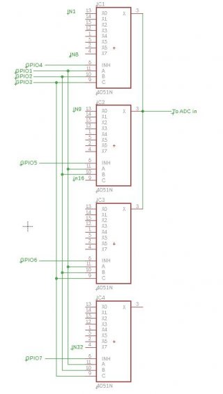
This is how I would wire the MUX chips
Capture.JPG

Without writing out all the code, here is how to do it (this is not the full program)
Code:
int MUXCHIPNUM = channelNumber/8;
int MUXCHANNEL =channelNumber % 8;

//To select the proper mux chip
// deselect all 4 MUX chips
DigitalWrite(GPIO4,HIGH);
DigitalWrite(GPIO5,HIGH);
DigitalWrite(GPIO6,HIGH);
DigitalWrite(GPIO7,HIGH);
// select the right one
switch (MUXCHANNUM) {
Case 0:DigitalWrite(GPIO4,LOW); break;
case 1:DigitalWrite(GPIO5,LOW); break;
Case 2:DigitalWrite(GPIO6,LOW); break;
Case 3:DigitalWrite(GPIO7,LOW); break;
}

// next select the proper mux channel
switch (MUXCHANNEL) {
case 0; 
digitalWrite(GPIO1,LOW);
digitalWrite(GPIO2,LOW);
digitalWrite(GPIO3,LOW);
digitalWrite(GPIO4,LOW);
break;
case 1; 
digitalWrite(GPIO1,HIGH);
digitalWrite(GPIO2,LOW);
digitalWrite(GPIO3,LOW);
digitalWrite(GPIO4,LOW);
break;
case 2; 
digitalWrite(GPIO1,LOW);
digitalWrite(GPIO2,HIGH);
digitalWrite(GPIO3,LOW);
digitalWrite(GPIO4,LOW);
break;
case 3; 
digitalWrite(GPIO1,HIGH);
digitalWrite(GPIO2,HIGH);
digitalWrite(GPIO3,LOW);
digitalWrite(GPIO4,LOW);
break;
case 4; 
digitalWrite(GPIO1,LOW);
digitalWrite(GPIO2,LOW);
digitalWrite(GPIO3,HIGH);
digitalWrite(GPIO4,LOW);
break;
case 5; 
digitalWrite(GPIO1,HIGH);
digitalWrite(GPIO2,LOW);
digitalWrite(GPIO3,HIGH);
digitalWrite(GPIO4,LOW);
break;
case 6; 
digitalWrite(GPIO1,LOW);
digitalWrite(GPIO2,HIGH);
digitalWrite(GPIO3,HIGH);
digitalWrite(GPIO4,LOW);
break;
case 7; 
digitalWrite(GPIO1,HIGH);
digitalWrite(GPIO2,HIGH);
digitalWrite(GPIO3,HIGH);
digitalWrite(GPIO4,LOW);
}

// after doing this mux selection, delay 10-100 us to allow the ADC input to settle before reading ADC
cheers
OOPS- I forgot to draw a line from IC4 X line to the X lines of the other 3
 
Back
Top