Custom Teensy 4.1 - Additional I/O Mapping Possible?

nemiro

Member
I have a custom Teensy 4.1 application that I am gearing up for. My application is very I/O intensive. I am looking at the possibility of multiplexing outputs, and I really do not want to do that, if possible. Given that this is custom, would it be possible to map additional I/O out of the processor, and add it into the definition files? Are there gotchas on this processor that might make that impractical? I looked over the schematics of Teensy 4.1 and the pinout of the processor, and (if I didn't miss something) this is what I see as being "open":

AD_B0: 00, 01
AD_B1: 00
SD_B1: 12-15
EMC: 00; 02-21; 30-39; 41

I don't need to map out all of those, but having another 10-20 GPIOs available would make for far fewer headaches in my design. I haven't looked at any special functions, like UARTS, etc. I might be missing something pretty big, so don't hesitate to let me know that.
 
Is this a DIY PCB where the 1062 will be used - or using the T_4.1 as manufactured?

For T_4.1: Which 'other' pins are in use? Noted on the card: there are a few unique signals on QSPI bottom pads and also those used for the SDIO SD card socket that could be used.

There is limited ability to bring pins out under the 1062 on the board as made - and all the ones brought out are present.

Though to make Ethernet it seems there were some many pins required for that - a dozen? - so a T_4.1 NE might have those pins on the unpopulated PHY chip pads. They won't be indicated on 'The Card' - but they will have some MCU connectivity for some number of them perhaps. And in some fashion, they are usable and software addressable.
 
This will be a DIY PCB, using the 1062, so I can bring out whatever signals are available to be used (physically).
 
For PJRC to get the needed pins on T_4.1 it took the larger 1062 chip to use the 6 layer board, IIRC.

Identifying the pins going to the PHY Ethernet might present ones already accounted for in the header files - if they have usable alternate MUX capabilities that could be used.
 
That's exactly the kind of information I'm looking for. I completely understand why there are not more of them brought out for the actual Teensy 4.1 board. The board would be enormous, to take all of them! In my case, I can find a home for almost every extra I/O.
 
If you want to use the extra pins with digitalWrite(), digitalRead(), pinMode(), you would edit core_pins.h.

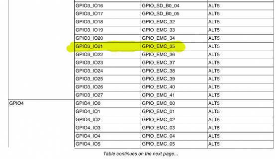
The one small gotcha is most of reference manual refers to GPIO1 to GPIO4 ports. There is an alternate set of registers called GPIO6 to GPIO9 which do the same thing, but they're on a faster bus. By default we configure the hardware to use GPIO6 to GPIO9. So if you look up a pin like EMC_35 in the reference manual, on page 302 is says you access it with GPIO3_IO21.

gpio.png

You would actually access this pin with GPIO8 bit 21. So in core_pins.h, you could add defines for bit 21 as expected and the register defines would all begin with "GPIO8" rather than "GPIO3".

Similarly, if you wanted to use analogWrite(), you'd edit pwm.c, for analogRead() edit analog.c, HardwareSerial.h, WireIMXRT.h, SPI.h, etc.

Of course you can always just access any hardware directly using its registers as documented in the reference manual. But often that involves a steep learning curve because many of the peripherals are loaded with a mind boggling number of features. NXP's documentation can sometimes be a little hard to digest.
 
No doubt on the mind boggling. I will try to read more this weekend. I want to sort this out before I begin laying out this portion of the schematics for the new board. Thank you for the help, and keep it rolling, if you think of other things.
 
I have been working with my hardware layout for quite a while, ad am at a stopping point for a bit. While here, I want to come up with a plan for the software end. With the time that has passed since I first asked the question on additional I/O, more questions have popped up for me. Before I ask those, I want to say that I am looking strictly for GPIO. I am not looking to map additional functions like serial ports, etc. Just simple I/O. First, my mapping (and yes, all my formatting of the columns has been lost):

Port Label Port Number Teensy/Arduino Pin Number
EMC_00 4.0 55
AD_B0_14 1.14 56
EMC_02 4.2 57
EMC_03 4.3 58
EMC_09 4.9 59
EMC_10 4.10 60
EMC_11 4.11 61
EMC_12 4.12 62
EMC_13 4.12 63
EMC_14 4.14 64
EMC_15 4.15 65
EMC_16 4.16 66
EMC_17 4.17 67
EMC_18 4.18 68
EMC_19 4.19 69
EMC_20 4.20 70
EMC_21 4.21 71
AD_B0_15 1.15 72
EMC_30 4.30 73
EMC_33 4.33 74
EMC_34 4.34 75
EMC_35 4.35 76
EMC_38 4.38 77
EMC_39 4.39 78
EMC_40 4.40 79
EMC_41 4.41 80
SD_B1_00 3.0 81
SD_B1_01 3.1 82
SD_B1_02 3.2 83
SD_B1_03 3.3 84
SD_B1_04 3.4 85
SD_B1_05 3.5 86
AD_B0_01 1.1 87
EMC_23 4.23 88
B0_04 2.4 89
B0_05 2.5 90
B0_06 2.6 91
B0_07 2.7 92
B0_08 2.8 93
B0_09 2.9 94

Believe it or not, my application uses all but 6 of these additional pins at the moment.

My questions are as follows:
1. Do I just modify the files in the LIB folder?
2. Do I modify what is there, or do I 'Save As' and give this a new device name (Teensy 4.1+, or something like that)?
3. Would this mess with Teensyduino?
4. Can I add a device to the Arduino/Teensyduino library?

Know this is pretty elementary for some here, but yes, I am very much clueless, so I am looking for some help. I have already procured the processors, and the PRJC bootloader chips for these. If this works, we'll build a lot of these :)

Thank you in advance for any help that can be offered!
 
You could do this many possible ways, but these are probably the most likely, in order of increasing difficulty.

1: Edit the core library files for pinMode(), digitalWrite(), digitalRead()

2: Copy and rename the pinMode(), digitalWrite(), digitalRead(), and edit that copy... eg: myPinMode(), myDigitalWrite(), myDigitalRead().

3: Create your own code using the hardware registers.

The downside to #1 is the possibility your edits could be overwritten and lost if you update or reinstall Teensyduino. Backup copies are essential. Of course, everyone doing creative work should use backup software for all their original irreplaceable data, but in practice many people don't go to the trouble. Just know that it is particularly important if you edit the core library files, because updates or reinstalling may overwrite them.

The first step is to simply find where these files are located on your computer. It varies depending on whether you use Windows, MacOS or Linux, and if you use Arduino 1.8.x or Arduino 2.0.x. The files are also on github, so for the rest of this message I'm going to link to the github files, but know you need to find the copy on your computer and edit those. File search may help. They may be located in folders which are normally hidden. On MacOS with Arduino 1.8.x, they are inside the application bundle, so control-click Arduino and "Show Package Contents" to look inside.

As a very first step, when you first edit the file add an intentional syntax error and click Verify in Arduino to make sure you get the error, as a confirmation you are editing the file Arduino is actually using.

The main pin definition file is core_pins.h.

https://github.com/PaulStoffregen/cores/blob/master/teensy4/core_pins.h

This file is large. It has 3 separate copies of the pin defines, for Teensy 4.0, Teensy 4.1 and MicroMod Teensy. Make sure you are editing in the correct area. Again, adding an intentional syntax error is the quick way to confirm you're editing in the right place. Do this first, because it's possible to waste a lot of time without results if you end up editing lines which aren't actually used.

For each pin you add, you'll need to know the native name and also which GPIO port and bit it is. You already know the native names. Use Table 10-1 in the reference manual. The native names to GPIO starts on page 300. The GPIO ports are 1-4. Teensy uses the fast version, which are 6-9, so you will need to add 5 to the number shown in Table 10-1.

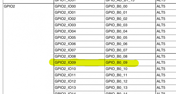
For example, if you edit the defines for Teensy 4.0 which have pins 0 to 39, and you wish to add pin "B0_09" as pin 40, you would first look it up in Table 10-1.
screenshot.png

You'll add 5, so for B0_09 the the GPIO is port 7, bit 9.

Then you'll edit the core_pins.h defines. First add the bit 9 part:

Code:
#define CORE_PIN37_BIT        12
#define CORE_PIN38_BIT        17
#define CORE_PIN39_BIT        16
[COLOR=#FF0000]#define CORE_PIN40_BIT        9[/COLOR]

Then for each of the register defines, add GPIO7. For example:

Code:
#define CORE_PIN37_PORTREG    GPIO8_DR
#define CORE_PIN38_PORTREG    GPIO8_DR
#define CORE_PIN39_PORTREG    GPIO8_DR
[COLOR=#FF0000]#define CORE_PIN40_PORTREG    GPIO7_DR[/COLOR]

Code:
#define CORE_PIN37_PORTSET    GPIO8_DR_SET
#define CORE_PIN38_PORTSET    GPIO8_DR_SET
#define CORE_PIN39_PORTSET    GPIO8_DR_SET
[COLOR=#FF0000]#define CORE_PIN40_PORTSET    GPIO7_DR_SET[/COLOR]

Several registers exist. Add this to the list for all of them.

Finally, you'll find 2 final groups of defines. Here you will add to the list using the pin name convention. For example:

Code:
#define CORE_PIN37_CONFIG    IOMUXC_SW_MUX_CTL_PAD_GPIO_SD_B0_00
#define CORE_PIN38_CONFIG    IOMUXC_SW_MUX_CTL_PAD_GPIO_SD_B0_05
#define CORE_PIN39_CONFIG    IOMUXC_SW_MUX_CTL_PAD_GPIO_SD_B0_04
[COLOR=#FF0000]#define CORE_PIN40_CONFIG    IOMUXC_SW_MUX_CTL_PAD_GPIO_B0_09[/COLOR]

You'll also need to edit the define for the number of pins, since you've increase from 40 to 41:

Code:
#define CORE_NUM_TOTAL_PINS    [COLOR=#FF0000]41[/COLOR]
#define CORE_NUM_DIGITAL       [COLOR=#FF0000]41[/COLOR]
#define CORE_NUM_INTERRUPT     [COLOR=#FF0000]41[/COLOR]
#define CORE_NUM_ANALOG        14
#define CORE_NUM_PWM           27

There are also redundant defines for the number of pins in pins_arduino.h. Edit those if your program or libraries you use need them.

Next you'll edit digital.c. It has a table which uses all those defines.

Code:
    {&CORE_PIN37_PORTREG, &CORE_PIN37_CONFIG, &CORE_PIN37_PADCONFIG, CORE_PIN37_BITMASK},
    {&CORE_PIN38_PORTREG, &CORE_PIN38_CONFIG, &CORE_PIN38_PADCONFIG, CORE_PIN38_BITMASK},
    {&CORE_PIN39_PORTREG, &CORE_PIN39_CONFIG, &CORE_PIN39_PADCONFIG, CORE_PIN39_BITMASK},
#if CORE_NUM_DIGITAL > 40
    {&CORE_PIN40_PORTREG, &CORE_PIN40_CONFIG, &CORE_PIN40_PADCONFIG, CORE_PIN40_BITMASK},
    {&CORE_PIN41_PORTREG, &CORE_PIN41_CONFIG, &CORE_PIN41_PADCONFIG, CORE_PIN41_BITMASK},
    {&CORE_PIN42_PORTREG, &CORE_PIN42_CONFIG, &CORE_PIN42_PADCONFIG, CORE_PIN42_BITMASK},
    {&CORE_PIN43_PORTREG, &CORE_PIN43_CONFIG, &CORE_PIN43_PADCONFIG, CORE_PIN43_BITMASK},
    {&CORE_PIN44_PORTREG, &CORE_PIN44_CONFIG, &CORE_PIN44_PADCONFIG, CORE_PIN44_BITMASK},
    {&CORE_PIN45_PORTREG, &CORE_PIN45_CONFIG, &CORE_PIN45_PADCONFIG, CORE_PIN45_BITMASK},
#endif
#if CORE_NUM_DIGITAL > 46
    {&CORE_PIN46_PORTREG, &CORE_PIN46_CONFIG, &CORE_PIN46_PADCONFIG, CORE_PIN46_BITMASK},
    {&CORE_PIN47_PORTREG, &CORE_PIN47_CONFIG, &CORE_PIN47_PADCONFIG, CORE_PIN47_BITMASK},
    {&CORE_PIN48_PORTREG, &CORE_PIN48_CONFIG, &CORE_PIN48_PADCONFIG, CORE_PIN48_BITMASK},
    {&CORE_PIN49_PORTREG, &CORE_PIN49_CONFIG, &CORE_PIN49_PADCONFIG, CORE_PIN49_BITMASK},
    {&CORE_PIN50_PORTREG, &CORE_PIN50_CONFIG, &CORE_PIN50_PADCONFIG, CORE_PIN50_BITMASK},
    {&CORE_PIN51_PORTREG, &CORE_PIN51_CONFIG, &CORE_PIN51_PADCONFIG, CORE_PIN51_BITMASK},
    {&CORE_PIN52_PORTREG, &CORE_PIN52_CONFIG, &CORE_PIN52_PADCONFIG, CORE_PIN52_BITMASK},
    {&CORE_PIN53_PORTREG, &CORE_PIN53_CONFIG, &CORE_PIN53_PADCONFIG, CORE_PIN53_BITMASK},
    {&CORE_PIN54_PORTREG, &CORE_PIN54_CONFIG, &CORE_PIN54_PADCONFIG, CORE_PIN54_BITMASK},
#endif
};

For this example, pin 40 already is in the table. The #if checks just keep the table from using extra space needlessly, so you can just ignore those unless you care about saving a small amount of memory. For beyond pin 54, you'll need to add more lines. But the hard work is already done in core_pins.h, so just copy and increase the numbers from 54 to 55.

Likewise, if you want the digitalWriteFast() and digitalReadFast() to be able to use pins beyond 54, you'll need to add them to those functions, which are in core_pins.h. For example:

Code:
                        } else if (pin == 45) {
                                CORE_PIN45_PORTSET = CORE_PIN45_BITMASK;
#endif
#if CORE_NUM_DIGITAL > 46
                        } else if (pin == 46) {
                                CORE_PIN46_PORTSET = CORE_PIN46_BITMASK;
                        } else if (pin == 47) {
                                CORE_PIN47_PORTSET = CORE_PIN47_BITMASK;
                        } else if (pin == 48) {
                                CORE_PIN48_PORTSET = CORE_PIN48_BITMASK;
                        } else if (pin == 49) {
                                CORE_PIN49_PORTSET = CORE_PIN49_BITMASK;
                        } else if (pin == 50) {
                                CORE_PIN50_PORTSET = CORE_PIN50_BITMASK;
                        } else if (pin == 51) {
                                CORE_PIN51_PORTSET = CORE_PIN51_BITMASK;
                        } else if (pin == 52) {
                                CORE_PIN52_PORTSET = CORE_PIN52_BITMASK;
                        } else if (pin == 53) {
                                CORE_PIN53_PORTSET = CORE_PIN53_BITMASK;
                        } else if (pin == 54) {
                                CORE_PIN54_PORTSET = CORE_PIN54_BITMASK;
[COLOR=#FF0000]                        } else if (pin == 55) {
                                CORE_PIN54_PORTSET = CORE_PIN54_BITMASK;[/COLOR]
#endif
                        }
                } else {
                        if (pin == 0) {
                                CORE_PIN0_PORTCLEAR = CORE_PIN0_BITMASK;
                        } else if (pin == 1) {
                                CORE_PIN1_PORTCLEAR = CORE_PIN1_BITMASK;

Like the table in digital.c, the hard work was already done so just copy line and increment the number.


For approach #2, you would do basically the same thing, but copy the code into files in your own program and change the global scope names so they don't conflict with the core library code.

For approach #3, you could craft whatever code you like.... creativity required. But hopefully this at least gives you some ideas?
 
Paul,
Thank you for putting this very thorough guide together. That was much more than I was expecting, and I am very appreciative of the time you put in on gathering all of this. Surely I won't be the only one to benefit from this?
 
OK, I have modified the files using method #1. I will call this the preliminary solution.View attachment core_pins.hView attachment digital.cView attachment pins_arduino.h

I now have several questions. Forgive my ignorance, as I write code well enough to be completely dangerous. I am wondering about a couple of things:
1. Instead of modifying the core library files, is it possible to break out these additional I/O definitions into a 'local' header file that I just include in my project? Not sure the compiler could handle that, but it would make it easier to keep track of the additional I/O files, and not risk them being overwritten

2. I can easily see reasons why #1 above will not work. Since I use both a 'regular' 4.1 and soon, this expanded version, can an additional definition be made that can be selected from a drop down within the IDE, to select this board? Would I then add the #if statements into these core library files like:
HTML:
#if CORE_NUM_DIGITAL > 54

or, would I just be better off switching the core library files back and forth as required?
 
I've been studying the reference manual all day. I'm trying to map my new pins 100-109 to 10 pads on the IC as follows:

100 = B1_04 = E12
101 = B1_05 = D12
102 = B1_06 = C12
103 = B1_07 = B12
104 = B1_08 = A12
105 = B1_09 = A13
106 = B1_10 = B13
107 = B1_11 = C13
108 = B1_14 = C14
109 = B1_15 = B14

I've created my own copy of the digital.c functions in deck_gpio.c:
Code:
#include "Arduino.h"
#include "deck_gpio.h"

const struct digital_pin_bitband_and_config_table_struct deck_digital_pin_to_info_PGM[] = {
  {&DECK_PIN100_PORTREG, &DECK_PIN100_CONFIG, &DECK_PIN100_PADCONFIG, DECK_PIN100_BITMASK},
  {&DECK_PIN101_PORTREG, &DECK_PIN101_CONFIG, &DECK_PIN101_PADCONFIG, DECK_PIN101_BITMASK},
  {&DECK_PIN102_PORTREG, &DECK_PIN102_CONFIG, &DECK_PIN102_PADCONFIG, DECK_PIN102_BITMASK},
  {&DECK_PIN103_PORTREG, &DECK_PIN103_CONFIG, &DECK_PIN103_PADCONFIG, DECK_PIN103_BITMASK},
  {&DECK_PIN104_PORTREG, &DECK_PIN104_CONFIG, &DECK_PIN104_PADCONFIG, DECK_PIN104_BITMASK},
  {&DECK_PIN105_PORTREG, &DECK_PIN105_CONFIG, &DECK_PIN105_PADCONFIG, DECK_PIN105_BITMASK},
  {&DECK_PIN106_PORTREG, &DECK_PIN106_CONFIG, &DECK_PIN106_PADCONFIG, DECK_PIN106_BITMASK},
  {&DECK_PIN107_PORTREG, &DECK_PIN107_CONFIG, &DECK_PIN107_PADCONFIG, DECK_PIN107_BITMASK},
  {&DECK_PIN108_PORTREG, &DECK_PIN108_CONFIG, &DECK_PIN108_PADCONFIG, DECK_PIN108_BITMASK},
  {&DECK_PIN109_PORTREG, &DECK_PIN109_CONFIG, &DECK_PIN109_PADCONFIG, DECK_PIN109_BITMASK},
};

#define DECK_START_DIGITAL  100
#define DECK_NUM_DIGITAL    (sizeof(deck_digital_pin_to_info_PGM) / sizeof(digital_pin_bitband_and_config_table_struct))

void deck_digitalWrite(uint8_t pin, uint8_t val)
{
  const struct digital_pin_bitband_and_config_table_struct *p;
  uint32_t pinmode, mask;

  pin -= DECK_START_DIGITAL;

  if (pin >= DECK_NUM_DIGITAL) return;
  p = deck_digital_pin_to_info_PGM + pin;
  pinmode = *(p->reg + 1);
  mask = p->mask;
  if (pinmode & mask) {
    Serial.print("Setting pin ");
    Serial.println(pin);
    // pin is configured for output mode
    if (val) {
      *(p->reg + 0x21) = mask; // set register
    } else {
      *(p->reg + 0x22) = mask; // clear register
    }
  } else {
    // pin is configured for input mode
    // value controls PULLUP/PULLDOWN resistors
    if (val) {
      *(p->pad) = IOMUXC_PAD_DSE(7) | IOMUXC_PAD_PKE | IOMUXC_PAD_PUE | IOMUXC_PAD_PUS(3) | IOMUXC_PAD_HYS;
    } else {
      *(p->pad) = IOMUXC_PAD_DSE(7) | IOMUXC_PAD_PKE | IOMUXC_PAD_PUE | IOMUXC_PAD_PUS(0) | IOMUXC_PAD_HYS;
    }
  }
}

void deck_digitalToggle(uint8_t pin)
{
  const struct digital_pin_bitband_and_config_table_struct *p;
  uint32_t mask;

  pin -= DECK_START_DIGITAL;

  if (pin >= DECK_NUM_DIGITAL) return;
  p = deck_digital_pin_to_info_PGM + pin;
  mask = p->mask;
  *(p->reg + 0x23) = mask; // toggle register
}

uint8_t deck_digitalRead(uint8_t pin)
{
  const struct digital_pin_bitband_and_config_table_struct *p;

  pin -= DECK_START_DIGITAL;

  if (pin >= DECK_NUM_DIGITAL) return 0;
  p = deck_digital_pin_to_info_PGM + pin;
  return (*(p->reg + 2) & p->mask) ? 1 : 0;
}

void deck_pinMode(uint8_t pin, uint8_t mode)
{
  const struct digital_pin_bitband_and_config_table_struct *p;

  pin -= DECK_START_DIGITAL;

  if (pin >= DECK_NUM_DIGITAL) return;
  p = deck_digital_pin_to_info_PGM + pin;
  if (mode == OUTPUT || mode == OUTPUT_OPENDRAIN) {
    Serial.println("Setting output");
    *(p->reg + 1) |= p->mask; // TODO: atomic
    if (mode == OUTPUT) {
      *(p->pad) = IOMUXC_PAD_DSE(7);
    } else { // OUTPUT_OPENDRAIN
      *(p->pad) = IOMUXC_PAD_DSE(7) | IOMUXC_PAD_ODE;
    }
  } else {
    *(p->reg + 1) &= ~(p->mask); // TODO: atomic
    if (mode == INPUT) {
      *(p->pad) = IOMUXC_PAD_DSE(7);
    } else if (mode == INPUT_PULLUP) {
      *(p->pad) = IOMUXC_PAD_DSE(7) | IOMUXC_PAD_PKE | IOMUXC_PAD_PUE | IOMUXC_PAD_PUS(3) | IOMUXC_PAD_HYS;
    } else if (mode == INPUT_PULLDOWN) {
      *(p->pad) = IOMUXC_PAD_DSE(7) | IOMUXC_PAD_PKE | IOMUXC_PAD_PUE | IOMUXC_PAD_PUS(0) | IOMUXC_PAD_HYS;
    } else { // INPUT_DISABLE
      *(p->pad) = IOMUXC_PAD_DSE(7) | IOMUXC_PAD_HYS;
    }
  }
  *(p->mux) = 5 | 0x10;
}

I've configured the pins in deck_gpio.h, based on Teensy's core_pins.h and created a mapping based on the unused pins in the spreadsheet from the post above. These should be on GPIO7 (GPIO2 in the docs):
Code:
#ifndef __DECK_GPIO_H__
#define __DECK_GPIO_H__

#include <core_pins.h>
#include <stdint.h>

#define DECK_PIN_START      100

void deck_digitalWrite(uint8_t pin, uint8_t val);
void deck_digitalToggle(uint8_t pin);
uint8_t deck_digitalRead(uint8_t pin);
void deck_pinMode(uint8_t pin, uint8_t mode);

#define DECK_PIN100_BIT       18
#define DECK_PIN101_BIT       19
#define DECK_PIN102_BIT       20
#define DECK_PIN103_BIT       21
#define DECK_PIN104_BIT       22
#define DECK_PIN105_BIT       23
#define DECK_PIN106_BIT       24
#define DECK_PIN107_BIT       25
#define DECK_PIN108_BIT       26
#define DECK_PIN109_BIT       27

#define DECK_PIN100_BITMASK     (1<<(DECK_PIN100_BIT))
#define DECK_PIN101_BITMASK     (1<<(DECK_PIN101_BIT))
#define DECK_PIN102_BITMASK     (1<<(DECK_PIN102_BIT))
#define DECK_PIN103_BITMASK     (1<<(DECK_PIN103_BIT))
#define DECK_PIN104_BITMASK     (1<<(DECK_PIN104_BIT))
#define DECK_PIN105_BITMASK     (1<<(DECK_PIN105_BIT))
#define DECK_PIN106_BITMASK     (1<<(DECK_PIN106_BIT))
#define DECK_PIN107_BITMASK     (1<<(DECK_PIN107_BIT))
#define DECK_PIN108_BITMASK     (1<<(DECK_PIN108_BIT))
#define DECK_PIN109_BITMASK     (1<<(DECK_PIN109_BIT))

#define DECK_PIN100_PORTREG     GPIO7_DR
#define DECK_PIN101_PORTREG     GPIO7_DR
#define DECK_PIN102_PORTREG     GPIO7_DR
#define DECK_PIN103_PORTREG     GPIO7_DR
#define DECK_PIN104_PORTREG     GPIO7_DR
#define DECK_PIN105_PORTREG     GPIO7_DR
#define DECK_PIN106_PORTREG     GPIO7_DR
#define DECK_PIN107_PORTREG     GPIO7_DR
#define DECK_PIN108_PORTREG     GPIO7_DR
#define DECK_PIN109_PORTREG     GPIO7_DR

#define DECK_PIN100_PORTSET     GPIO7_DR_SET
#define DECK_PIN101_PORTSET     GPIO7_DR_SET
#define DECK_PIN102_PORTSET     GPIO7_DR_SET
#define DECK_PIN103_PORTSET     GPIO7_DR_SET
#define DECK_PIN104_PORTSET     GPIO7_DR_SET
#define DECK_PIN105_PORTSET     GPIO7_DR_SET
#define DECK_PIN106_PORTSET     GPIO7_DR_SET
#define DECK_PIN107_PORTSET     GPIO7_DR_SET
#define DECK_PIN108_PORTSET     GPIO7_DR_SET
#define DECK_PIN109_PORTSET     GPIO7_DR_SET

#define DECK_PIN100_PORTCLEAR GPIO7_DR_CLEAR
#define DECK_PIN101_PORTCLEAR GPIO7_DR_CLEAR
#define DECK_PIN102_PORTCLEAR GPIO7_DR_CLEAR
#define DECK_PIN103_PORTCLEAR GPIO7_DR_CLEAR
#define DECK_PIN104_PORTCLEAR GPIO7_DR_CLEAR
#define DECK_PIN105_PORTCLEAR GPIO7_DR_CLEAR
#define DECK_PIN106_PORTCLEAR GPIO7_DR_CLEAR
#define DECK_PIN107_PORTCLEAR GPIO7_DR_CLEAR
#define DECK_PIN108_PORTCLEAR GPIO7_DR_CLEAR
#define DECK_PIN109_PORTCLEAR GPIO7_DR_CLEAR

#define DECK_PIN100_PORTTOGGLE  GPIO7_DR_TOGGLE
#define DECK_PIN101_PORTTOGGLE  GPIO7_DR_TOGGLE
#define DECK_PIN102_PORTTOGGLE  GPIO7_DR_TOGGLE
#define DECK_PIN103_PORTTOGGLE  GPIO7_DR_TOGGLE
#define DECK_PIN104_PORTTOGGLE  GPIO7_DR_TOGGLE
#define DECK_PIN105_PORTTOGGLE  GPIO7_DR_TOGGLE
#define DECK_PIN106_PORTTOGGLE  GPIO7_DR_TOGGLE
#define DECK_PIN107_PORTTOGGLE  GPIO7_DR_TOGGLE
#define DECK_PIN108_PORTTOGGLE  GPIO7_DR_TOGGLE
#define DECK_PIN109_PORTTOGGLE  GPIO7_DR_TOGGLE

#define DECK_PIN100_DDRREG      GPIO7_GDIR
#define DECK_PIN101_DDRREG      GPIO7_GDIR
#define DECK_PIN102_DDRREG      GPIO7_GDIR
#define DECK_PIN103_DDRREG      GPIO7_GDIR
#define DECK_PIN104_DDRREG      GPIO7_GDIR
#define DECK_PIN105_DDRREG      GPIO7_GDIR
#define DECK_PIN106_DDRREG      GPIO7_GDIR
#define DECK_PIN107_DDRREG      GPIO7_GDIR
#define DECK_PIN108_DDRREG      GPIO7_GDIR
#define DECK_PIN109_DDRREG      GPIO7_GDIR

#define DECK_PIN100_PINREG      GPIO7_PSR
#define DECK_PIN101_PINREG      GPIO7_PSR
#define DECK_PIN102_PINREG      GPIO7_PSR
#define DECK_PIN103_PINREG      GPIO7_PSR
#define DECK_PIN104_PINREG      GPIO7_PSR
#define DECK_PIN105_PINREG      GPIO7_PSR
#define DECK_PIN106_PINREG      GPIO7_PSR
#define DECK_PIN107_PINREG      GPIO7_PSR
#define DECK_PIN108_PINREG      GPIO7_PSR
#define DECK_PIN109_PINREG      GPIO7_PSR

#define DECK_PIN100_CONFIG      IOMUXC_SW_MUX_CTL_PAD_GPIO_B1_04
#define DECK_PIN101_CONFIG      IOMUXC_SW_MUX_CTL_PAD_GPIO_B1_05
#define DECK_PIN102_CONFIG      IOMUXC_SW_MUX_CTL_PAD_GPIO_B1_06
#define DECK_PIN103_CONFIG      IOMUXC_SW_MUX_CTL_PAD_GPIO_B1_07
#define DECK_PIN104_CONFIG      IOMUXC_SW_MUX_CTL_PAD_GPIO_B1_08
#define DECK_PIN105_CONFIG      IOMUXC_SW_MUX_CTL_PAD_GPIO_B1_09
#define DECK_PIN106_CONFIG      IOMUXC_SW_MUX_CTL_PAD_GPIO_B1_10
#define DECK_PIN107_CONFIG      IOMUXC_SW_MUX_CTL_PAD_GPIO_B1_11
#define DECK_PIN108_CONFIG      IOMUXC_SW_MUX_CTL_PAD_GPIO_B1_14
#define DECK_PIN109_CONFIG      IOMUXC_SW_MUX_CTL_PAD_GPIO_B1_15

#define DECK_PIN100_PADCONFIG IOMUXC_SW_PAD_CTL_PAD_GPIO_B1_04
#define DECK_PIN101_PADCONFIG IOMUXC_SW_PAD_CTL_PAD_GPIO_B1_05
#define DECK_PIN102_PADCONFIG IOMUXC_SW_PAD_CTL_PAD_GPIO_B1_06
#define DECK_PIN103_PADCONFIG IOMUXC_SW_PAD_CTL_PAD_GPIO_B1_07
#define DECK_PIN104_PADCONFIG IOMUXC_SW_PAD_CTL_PAD_GPIO_B1_08
#define DECK_PIN105_PADCONFIG IOMUXC_SW_PAD_CTL_PAD_GPIO_B1_09
#define DECK_PIN106_PADCONFIG IOMUXC_SW_PAD_CTL_PAD_GPIO_B1_10
#define DECK_PIN107_PADCONFIG IOMUXC_SW_PAD_CTL_PAD_GPIO_B1_11
#define DECK_PIN108_PADCONFIG IOMUXC_SW_PAD_CTL_PAD_GPIO_B1_14
#define DECK_PIN109_PADCONFIG IOMUXC_SW_PAD_CTL_PAD_GPIO_B1_15


#endif // __DECK_GPIO_H__

Now I'm trying to test by toggling one pin at a time each minute, so I can test with probes. But this isn't working. The pins appear to be floating when toggled high and low. Anyone see anything wrong with the mapping? It is indeed mind blowing. Is the Ethernet chip on the Teensy 4.1 configured automatically at boot time? It would normally use some of those pins, but I did not include the Ethernet IC in my design. I'm hoping to use them as GPIOs.

Code:
#include "deck_gpio.h"

void setup() {
  // put your setup code here, to run once:

  Serial.begin(115200);

  pinMode(13, OUTPUT);
  
  for (int x = 100; x < 110; x++) {
    deck_pinMode(x, OUTPUT);
    deck_digitalWrite(x, LOW);
  }
}

void loop() {

  char *pins[] = { 
    "R3",
    "R2",
    "C1",
    "C3",
    "C4",
    "C2",
    "C0",
    "R0",
    "R1",
    "R4"
  };
  
  for (int x = 100; x < 110; x++) {
    
    Serial.print("Setting GPIO");
    Serial.println(x);
    
    deck_digitalWrite(x, HIGH);
    for (int y = 0; y < 30; y++) {
      Serial.println(pins[x-100]);
      delay(1000);
      digitalWrite(13, HIGH);
      delay(1000);
      digitalWrite(13, LOW);
    }
    deck_digitalWrite(x, LOW);
  }
 
I'm not sure why this code isn't working. But I can at least answer this:

Is the Ethernet chip on the Teensy 4.1 configured automatically at boot time?

No, the ethernet PHY chip isn't configured at boot. It doesn't get any configuration at all unless you run one of the libraries which use it.
 
Thanks Paul! I think I got it working. I arbitrarily picked those bits on GPIO7, not realizing that there were limitations on what pins can map to what bits. I used the MCUXpresso pins tool to build a configuration matching what I need.

https://mcuxpresso.nxp.com/en/pins

That clearly showed me that the mappings I had were not allowed. I updated my bits to reflect what the pins tool allowed me to configure. Here's are the bits I ended up with...

Code:
#define DECK_PIN100_BIT       20
#define DECK_PIN101_BIT       21
#define DECK_PIN102_BIT       22
#define DECK_PIN103_BIT       23
#define DECK_PIN104_BIT       24
#define DECK_PIN105_BIT       25
#define DECK_PIN106_BIT       26
#define DECK_PIN107_BIT       27
#define DECK_PIN108_BIT       30
#define DECK_PIN109_BIT       31
 
The pins tool linked above was the cat's meow if you get confused like I did. It even gives you example code.
 
Back
Top