5V 3V3 VUSB power supply struggles - Teensy4.1 - what kills my NCV8186AMN330TAG ics?

sicco

Well-known member
A couple of annoying Teensy 4.1 hardware failures recently. I have a theory on what kills them, I think I have the mitigation. But can someone confirm I'm on the right track?

A board with a Teensy 4.1 on it is supplied by USB 5V. The board has many sensor chips that all are supplied by the Teensy 3V3 output. All sensor chips have bypass caps, 10uF each, there are 10+. So I have 100+ uF capacitance on the 3V3 rail.
The problem is that the Teensy 3V3 regulator IC fails occasionally. As in it dies. With the Teensy 5V fuse blowing also sometimes.

The 5V VUSB also powers several DCDC isolators on my board. Those typically draw 100-200 mA collectively. So they are an extra load on the 5V rail, also when I unplug USB because they sit on the Teensy VIN (=VUSB) pins.

My theory is that when I unplug the Teensy USB port, I get excessive reverse current in the 3V3 regulator IC (NCV8186AMN330TAG in my case). So the caps on the 3V3 rail discharging through that LDO regulator, back towards the 5V rail. Datasheet NCV8186AMN330TAG hints that ''Reverse Current - The PMOS pass transistor has an inherent body diode which will be forward biased in the case when VOUT > VIN. Due to this fact in cases, where the extended reverse current condition can be anticipated the device may require additional external protection. ". So I guess an extra diode from 3V3 (anode) back to 5V (cathode) so that the discharge current from the 3V3 rails will no longer be able to kill it. Does that make sense?

Stated differently: is there a spec for the max external capacitance on the Teensy 3V3 pin - when there's also significant load that keeps draining the 5V rail when the 5V supply (from USB) suddenly disappears?
 
I think you are on the right track. The LDO datasheet does mention the need for additional protection in the case of extended reverse current conditions when Vout > Vin to protect the output pass transistor.

A flyback diode would seem to provide that protection and would be what I would try.

There are occasional reports of the 3.3V LDO failing on the forum which always seemed odd to me since the parts are well protected against output shorts, thermal and the like. Perhaps you are pointing to a potential failure mechanism in some applications that has been somewhat overlooked.
 
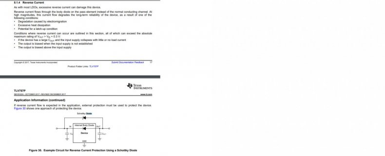
The TI datasheet for the TLV75733 that was used in earlier Teensy4.1's is more specific about what apparently is a generic electrical design problem:

TI_TLV757datasheet.jpg

So from now on, I better add that same Schottkey diode from 3V3 to VIN, by default, to all boards that use a Teensy4.1... Also because the TI and the Diodes datasheets leave us clueless on what Cout value on the 3V3 rail constitutes a serious threat. It might be the 4u7 that all Teensies41 have already... Or maybe it is only biting at 50 uF. Or 100 uF. Who knows... Seems to depend also on how much current the Teensy draws when the VIN voltage disappears. And how sudden the VIN disappears. And how much the VIN/VUSB/+5V rail/pin is loaded with other devices that sink a LDO reverse current... The TI datasheet wording "...this current flow degrades the long-term reliability of the device, as a result of one of the following conditions: • Degradation caused by electromigration..." That's almost as if they say yeah that may kill your product eventually, maybe, maybe not, but, just give it a go and see if it's after 1, 10 or 100 years before it strikes...
 
I have never noticed that reverse current warning with old-school LDO regulators nor have I ever heard of that type of failure issue with those. Many people, myself included, have certainly hung thousands of uF off those without incident or special protection.

From the link below it appears that there are design tradeoffs that are made at the chip level to minimize drop-out voltage but that also increases the risk of reverse current failure. I'll certainly think twice before I spec an LDO simply because it has an ultra low dropout unless it is key to the application. There might also be some physical tradeoffs being made to fit into the latest tiny packages.

Here is a good overview from TI of the issue and various approaches to solving that I ran across. Your Schottky diode approach still looks like the way to go. https://e2e.ti.com/blogs_/b/powerhouse/posts/ldo-basics-preventing-reverse-current-in-ldos
 
Any success on adding this reverse diode?
We have also had some failures with the NCV8186AMN330TAG.
Looking at the datasheet, Teensy fails on the input capacitance requirement of at least 1uF close to the IC.
I am thinking more on an instability issue, caused by this lack of capacitance.
The reverse current should be blocked by the P-chl FET in series, therefore I do not see any added value in placing the suggested reverse diode.
 
Good point about the reverse current MOSFET on the input side. That should prevent any current that would backflow to the power source, but perhaps there is a sneak path for current through the USB1/2_VBUS inputs on the RT1060? It looks like those inputs might power an on-chip 3.3V regulator.

Having light capacitance on the input side may affect stability, but I doubt that would lead to failure of the part, just poor regulation perhaps?
 
Any success on adding this reverse diode?
We have also had some failures with the NCV8186AMN330TAG.
Looking at the datasheet, Teensy fails on the input capacitance requirement of at least 1uF close to the IC.
I am thinking more on an instability issue, caused by this lack of capacitance.
The reverse current should be blocked by the P-chl FET in series, therefore I do not see any added value in placing the suggested reverse diode.

After adding the extra diode from the Teensy4.1 3v3 to the 5v rail, the NCV8186AMN330TAG T41 LDO survived. As mentioned above, this board design had:
a) a lot of extra low ESR capacitors on its Teensy 3v3 LDO output pin, and,
b) a parallel low ohm load on its 5v input pin. 3 isolated DCDC converters that drain ~200 mA from the 5v rail.
That combination appeared to be fatal for the 8 pin LDO on the T41. Fatal when the 5v supply is suddenly cut. For example when unplugging the micro USB cable.
 
The reverse current is blocked by the P-FET Q1, so the parallel load on the 5V input pin should not be a problem.
Only thing I can imagine on cutting the 5V supply is a peak voltage over the input pin, caused by the connecting inductance.
But also in that case I do not understand why a reverse diode helps protecting.

Did you have any fails with the earlier TI part TLV75733P?
In the datasheet of this TLV75733P the same requirements are mentioned, also at least 1uF at the input and a reverse current protection.

Q1 I think is good for protecting against reverse polarity on the VIN input, but i don’t think it necessarily stops reverse current flow. As long as Vgs is negative enough, the FET channel is low ohmic and thus conducts.

I think I only had serious trouble with the newer 8 pins LDOs. So not with the 6 pin TLV75733.
 
You are right, it keeps indeed conducting as long as the 5V supply is higher than -VGS(th), DMG2305UX mentions minimal 0.5V. Now I understand why the diode does its job, thanks for explaining.
We will also add a Schottky in reverse over the NCV8186AMN330TAG, hope that helps.
Last year we had 2 defects over the about 50pc Teensy 4.1 we use, not much, but within a year we should notice the difference.
 
a) a lot of extra low ESR capacitors on its Teensy 3v3 LDO output pin, and,
b) a parallel low ohm load on its 5v input pin. 3 isolated DCDC converters that drain ~200 mA from the 5v rail.

Could you be more specific about these particular capacitors and DCDC converters, and the loads connected to the converters? In other words, if I were to attempt to reproduce this problem, which parts would I need to buy? Can you give me another other relevant details about how they're connected, like wire lengths, PCB, etc?
 
Last edited:
I should mention, since March 2023, all new Teensy 4.1 are built with TLV75533P.

OnSemi NCV8186AMN330TAG was used for about 1 year while semiconductor shortages impacted the supply of Texas Instruments voltage regulators. During this time we discovered this part does not actually have soft start, as OnSemi's datasheet claims, which was the main reason we switched back to TI. Knowing this now, I'm a little skeptical about everything else OnSemi says in their datasheet.

As the shortages eased up, TLV75533P became available before TLV75733P. I did quite a lot of side-by-side testing. They have nearly identical performance. Their datasheets have almost all the same specs, except max current and drop out voltage (which is specified as 425mV @ 1A versus 238mV @ 0.5A),and actual testing showed the dropout was pretty much identical at 100 to 180mA normally used by Teensy 4.1. I strongly suspect these 2 TI parts have identical silicon with the current limit somehow configured differently. Testing showed that using more than about 500 mA with 5V input and Teensy 4.1's 6 layer PCB (using large vias to couple heat to 2 ground plane internal layers) really isn't feasible due to thermal limiting. We went with TLV75533P because we really wanted to get back to proper soft start.
 
Good to hear the onsemi part is abandoned, that should avoid this problem in the future.
I wonder why is chosen for the P-FET as reverse polarity protection, instead of a Schottky in series, that protects next to reverse polarity also for reverse current through the LDO.
Extra benifit will be a more equal power distribution over two parts.
 
I wonder why is chosen for the P-FET as reverse polarity protection, instead of a Schottky in series,

USB host was the main motivation. Many but not all USB devices handle less than 5 volts pretty well, but most unpowered USB hubs tend to be quite problematic.

Ability to (just barely, LDO regulator on the edge of dropout) run from 3.6 volt Lithium Ion batteries was also a goal.

Feedback from years of Teensy 3.6 shows the diode forward voltage drop really impacted these applications.


Good to hear the onsemi part is abandoned

Indeed, I'm still pretty unhappy about the lack of soft start, which OnSemi's datasheet erroneously claims it has. At least a couple people reported the inrush current disrupting DCDC converters they used with earlier Teensy 4.1 boards with the original TI chip.

I do have some boards still here with the OnSemi chip. Really hoping to get details on the specific capacitors and DCDC parts and their approximate loads. I'm reluctant to blame OnSemi without actually running tests on my own workbench. But given the dishonest info about soft start, I wouldn't be too surprised if that chip turns out to have other unanticipated problems.

But in late 2021, there simply weren't very many LDO chips on the entire market. NCV8186AMN330TAG, at least on paper, checked all the requirements, and we were able to buy enough to keep Teensy 4.1 (mostly) available throughout the semiconductor shortage time. I did do testing on my workbench, but mostly for dropout voltage and thermal performance. I didn't test soft start. I didn't do tests like excessive added capacitance. Not sure how much time I'll dedicate to NCV8186AMN330TAG, but curious to do these tests with the TI part just to check where we're at and perhaps update the web page with better guidance on power connections.
 
Could you be more specific about these particular capacitors and DCDC converters, and the loads connected to the converters? In other words, if I were to attempt to reproduce this problem, which parts would I need to buy? Can you give me another other relevant details about how they're connected, like wire lengths, PCB, etc?

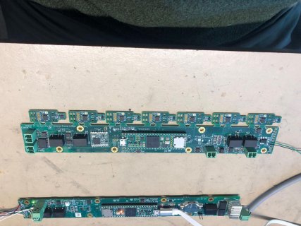
The DC-DC converters on the 5V VIN rail were 4 x ISE0505A by XP, two of which draw 100 mA both on their isolated outputs. The other two draw less, say 30 mA ish.
The decoupling caps on the 3V rail (that I labelled low ESR) were 10uF 0603 -whatever JLCPCB selected there- ( // 100 nF), 8 in parallel, one nearby each ST MEMS sensor chip of which the board had 7. So I guess ~100 uF in total on the 3V rail.
Plus on the 3V rail whatever there is on a RFM95W-868S2 radio module. Plus what's on the Teensy itself.

The 5V rail had ~30 uF of the same type of SMD caps.

Multilayer board with decent GND, 5V and 3V planes.

IMG_6004.jpg
 
Back
Top