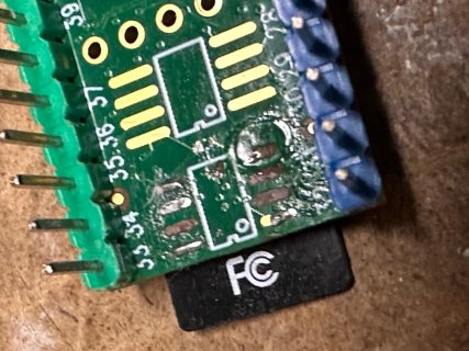
Are the PSRAM contacts on my 4.1 board beyond repair?

IMG_1977.jpg

Long story short, I tried surface mounting additional PSRAM onto my Teensy 4.1 without having the requisite soldering skills to do so. As you can imagine, this resulted in the additional PSRAM not being recognized, and I threw the chip out.

I now would like to try again, as I have another compatible PSRAM chip from the PJRC store, however my questions are:

  1. The outter-most PSRAM slot is totally FUBAR, right? I can't imagine how I'd be able to make current flow between the chip and the board
  2. Does that mean that I simply won't be able to use the inner slot whatsoever?
That's okay if so, that information was clearly documented so I'm ready to accept this 'L' due to my own obvious errors. I just want to make sure, there's no way to use the inner slot by itself, correct?

Thanks in advance!
 
Is only a single QSPI/PSRAM chip needed?

Most of those pads look awful. As long as they aren't shorted there might be a way to get one PSRAM working.

refer to the T_4.1 card and get the orientation right ...
The single pad near pin #32 looks like the only usable one - that is CS0 that defines the first PSRAM.

> All the other 7 pins to those chips are common.

With a proper soldering job on the second set of pads EXCEPT CS1 not soldered or touching the pad. With that PSRAM leg carefully bent up perhaps.

Then getting a fine wire soldered from CS0 to that leg on the PSRAM where CS1 is not soldered.


But the soldering would need to be much better - especially managing the short thin wire from the chip leg top the pad. With the pins in that isn't the easiest.

Extra flux helps the solder flow and better heat transfer - but needs to be washed clean when done.
 
Back
Top