I set it to 1 and skipped 133 as I figured there was no point in testing it - we know it worksOdd though it should have a line for 133 MHz if the downloaded sketch LINE#1 wasn't changed from: #define FIRST_SPEED 0
You are using an out of date browser. It may not display this or other websites correctly.
You should upgrade or use an alternative browser.
You should upgrade or use an alternative browser.
Call to arms | Teensy + SDRAM = true
- Thread starter Dogbone06
- Start date
defragster
Senior Member+
As for the problems at MCU F_CPU over 600 MHz - perhaps it is these likely these ns_to_clocks() timing based values not adjusting for enhanced F_CPU_ACTUAL clock rates so recovery times are being violated ?
Glad the edit made sense with the set of adjustments that evolved to get the test where it is.
Did a quick edit for CSV printed table output. But doesn't cut and paste into excel or forum without save as CSV and then open in XL and edit the 'Read Err' column to not use exponents, and edit column justify - then it cuts/pastes from XL as below - except doesn't have the 'pF used marker' to indicate 'No CAP' or the value used.
Code:
    // configure SDRAM parameters
    SEMC_BR0 = 0x80000000 | SEMC_BR_MS(13 /*13 = 32 Mbyte*/) | SEMC_BR_VLD;
    SEMC_SDRAMCR0 = SEMC_SDRAMCR0_CL(3) |
        SEMC_SDRAMCR0_COL(3) |  // 3 = 9 bit column
        SEMC_SDRAMCR0_BL(3) |   // 3 = 8 word burst length
        SEMC_SDRAMCR0_PS;       // use 16 bit data
    SEMC_SDRAMCR1 =
        SEMC_SDRAMCR1_ACT2PRE((ns_to_clocks(42, freq)-1)) | // tRAS: ACTIVE to PRECHARGE
        SEMC_SDRAMCR1_CKEOFF((ns_to_clocks(42, freq)-1)) |  // self refresh
        SEMC_SDRAMCR1_WRC((ns_to_clocks(12, freq)-1)) |     // tWR: WRITE recovery
        SEMC_SDRAMCR1_RFRC((ns_to_clocks(67, freq)-1)) |    // tRFC or tXSR: REFRESH recovery
        SEMC_SDRAMCR1_ACT2RW((ns_to_clocks(18, freq)-1)) |  // tRCD: ACTIVE to READ/WRITE
        SEMC_SDRAMCR1_PRE2ACT((ns_to_clocks(18, freq)-1));  // tRP: PRECHARGE to ACTIVE/REFRESH
    SEMC_SDRAMCR2 = 0; // TODO... page 1425
    SEMC_SDRAMCR3 = 0; // TODO...page 1426
    SEMC_SDRAMCR2 =
        SEMC_SDRAMCR2_SRRC((ns_to_clocks(67, freq) - 1)) |
        SEMC_SDRAMCR2_REF2REF(ns_to_clocks(60, freq)) |           /* No Minus one to keep with RM */
        SEMC_SDRAMCR2_ACT2ACT(ns_to_clocks(60, freq)) | /* No Minus one to keep with RM */
SEMC_SDRAMCR2_ITO(0); //sdk has: idle = config->tIdleTimeout_Ns / config->tPrescalePeriod_NsVery good - except for the shock it caused here - That was put in so we know that we know it works.I set it to 1 and skipped 133 as I figured there was no point in testing it - we know it works
Glad the edit made sense with the set of adjustments that evolved to get the test where it is.
Did a quick edit for CSV printed table output. But doesn't cut and paste into excel or forum without save as CSV and then open in XL and edit the 'Read Err' column to not use exponents, and edit column justify - then it cuts/pastes from XL as below - except doesn't have the 'pF used marker' to indicate 'No CAP' or the value used.
| Test summary: 57 tests with 5 ReReads at F_CPU_ACTUAL 600 Mhz: | |||
| MHz | Seconds | Read Err | % Err |
| 133 | 160 | 0 | 0 |
| 166 | 145 | 0 | 0 |
| 196 | 136 | 0 | 0 |
| 206 | 133 | 0 | 0 |
| 216 | 132 | 0 | 0 |
| 227 | 128 | 0 | 0 |
| 240 | 127 | 0 | 0 |
| 254 | 124 | 937,185 | 0.0392 |
| 270 | 122 | 1,388,401,790 | 58.0738 |
Those values use SEMC clock ticks as units, they don't care about the CPU's clock.As for the problems at MCU F_CPU over 600 MHz - perhaps it is these likely these ns_to_clocks() timing based values not adjusting for enhanced F_CPU_ACTUAL clock rates so recovery times are being violated ?
mjs513
Senior Member+
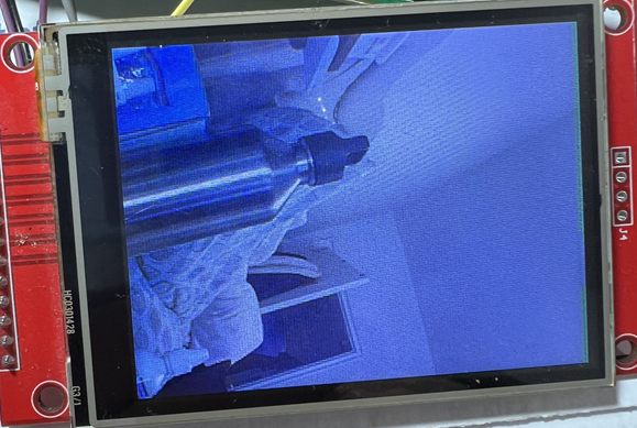
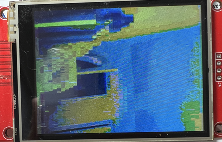
Just by way of an update @KurtE got the OV7670 and OV7670 video working using the micromod as the test platform. If you try it on the SDRAM something strange is going on.
If you use DMAMEM for the framebuffers image is perfect

if you use EXTMEM with __attribute__((aligned(32))); not so good

not sure what issue is with SDRAM - did try the approach earlier the way GIGA uses SDRAM and no good, tried with making the entire region MEM_NOCACHE and again made it worse.
Maybe a strange interaction between DMA and SDRAM.
Cheers. Will have to try with CSI at some point but other cameras await.
If you use DMAMEM for the framebuffers image is perfect
if you use EXTMEM with __attribute__((aligned(32))); not so good
not sure what issue is with SDRAM - did try the approach earlier the way GIGA uses SDRAM and no good, tried with making the entire region MEM_NOCACHE and again made it worse.
Maybe a strange interaction between DMA and SDRAM.
Cheers. Will have to try with CSI at some point but other cameras await.
KurtE
Senior Member+
not sure what issue is with SDRAM - did try the approach earlier the way GIGA uses SDRAM and no good, tried with making the entire region MEM_NOCACHE and again made it worse.
But when I looked at their schematic their SDRam setup looks very different than what I believe you are doing on these dev boards.
That is they are using 12 address pins and 16 data pins to talk to the SDRAM.
Has anyone tried adding this type of SDRam to the IMXRT boards? My quick look through the SEMC chapter (24) of the RM, and at least with my quick look, I think they might support something like this. But again, I only glanced at the RM on this.
defragster
Senior Member+
Okay, Thanks. Something else then ... MCU cycling faster and leaving the SDRAM behind it seems ...Those values use SEMC clock ticks as units, they don't care about the CPU's clock.
Im sure you’re already doing this - but you are flushing cache?not sure what issue is with SDRAM - did try the approach earlier the way GIGA uses SDRAM and no good, tried with making the entire region MEM_NOCACHE and again made it worse.
Maybe a strange interaction between DMA and SDRAM.
Maybe try do a data integrity test with SDRAM/DMA? Copy data from one buffer to another and see if they are identical ?
mjs513
Senior Member+
yepIm sure you’re already doing this - but you are flushing cache?
Maybe try do a data integrity test with SDRAM/DMA? Copy data from one buffer to another and see if they are identical ?
Code:
DMAMEM uint16_t array1[(320) * 240] __attribute__((aligned(32)));
EXTMEM uint16_t array2[(320) * 240] __attribute__((aligned(32)));

int errorCnt = 0;
int arraySize = (320 * 240);

void setup() {
  Serial.begin(115200);
   while (!Serial && millis() < 4000)
    ;

  if (CrashReport) {
    Serial.print(CrashReport);
    Serial.print("Any Key to continue ...");
    delay(50);
    while (1) {
      if ( Serial.available() ) break;
      asm ("wfi");
    }
    while ( Serial.available() ) {
      Serial.print((char)Serial.read());
    }
  }

  Serial.println("Memory comparison test");
  Serial.println("Initializing Array1");
  for(int i = 0; i < arraySize; i++) {
    array1[i] = random(255);
  }
  Serial.println("Copy Array 1 to Array2");
  for(int i = 0; i < arraySize; i++) {
    array2[i] = array1[i];
  }
  Serial.println("comparing Arrays");
  for(int i = 0; i < arraySize; i++) {
    if(array2[i] != array1[i]) errorCnt = errorCnt + 1;
  }
  Serial.printf("DMA to SDRAM Error Count for %d array comparison: %d\n", arraySize, errorCnt);

}

void loop() {

}
Code:
Memory comparison test
Initializing Array1
Copy Array 1 to Array2
comparing Arrays
DMA to SDRAM Error Count for 76800 array comparison: 0KurtE
Senior Member+
I will try to get back to trying it on this board. Sort of a PIA at times to hook up all of the wires in a secure enough way. So I much easier playing using the other boards.Assuming the camera stuff is uslng FlexIO and DMA to move from shifter registers to RAM... are the shifters signalling any errors, to indicate overruns (new data being placed without the old data being read first) ?
Did find using my camera shifter boards I did during the T4.1 stuff is coming in handy as it could plug into the T4.1 board, camera plugs into it and spare connector to allow me to setup Logic Analyzer.
I had two of them I had not assembled, so will do that and try again on devboard...
What I should have done, was setup a simple converter board to make it easy to plug camera in and plug the adapter into breadboard...
Something like:
Probably won't order any yet...
mjs513
Senior Member+
Sorry been distracted today for a bunch of reasons. Reran the tests but added the time to copy the arrayAnd with a DMA transfer?
Code:
DMAMEM to EXTMEM: 0 errors, 1010 microseconds to copy
DMAMEM to DMAMEM: 0 errors,  319 microseconds to copy
RAMMEM to RAMMEM: 0 errors,   68 microseconds to copy
RAMMEM to RAMMEM: 0 errors,  257 microseconds to copy
RAMMEM to EXTMEM: 0 errors,  470 microseconds to copy
EXTMEM to DMAMEM: 0 errors, 1294 microseconds to copy
Saw the same type of times when I tried using PXP to rotate an image. If EXTMEM was involved it was on the order of 1300 microseconds, when DMAMEM or RAM it was on the order of 600 microseconds.
Cheers.
EDIT for extmem to dmamem
Code:
SDRAM clock   time to transfer (micros)
       133                   1513
       166                   1294
       198                   1149
       206                   1272
       216                   1272
       anything above this fails (I have no cap on the board)
Interesting that 198mhz is the minimum.
Last edited:
defragster
Senior Member+
I made quick note somewhere on past pages with initial speed results showing longer at faster - but not seen with current test.Interesting that 198mhz is the minimum.Code:SDRAM clock time to transfer (micros) 133 1513 166 1294 198 1149 206 1272 216 1272 anything above this fails (I have no cap on the board)
Another thing the 'OneScanCap.ino' occasionally shows is an added 3 seconds to all times across the tests between one build and another?
> like p# 871 .vs. 873 {EDIT: Note @Rezo #872 matches one result but not the other as well}
Last edited:
Meanwhiles, for anyones enjoyment, here is a video of a music player demo running on LVGL v9.0.0
I think there is a lot of room left to optimize.
It has two screen sized frame buffers (1.3Mb each) that LVGL writes into, and the eLCDIF reads from the ready buffer while the other is being written to.
I think there is a lot of room left to optimize.
It has two screen sized frame buffers (1.3Mb each) that LVGL writes into, and the eLCDIF reads from the ready buffer while the other is being written to.
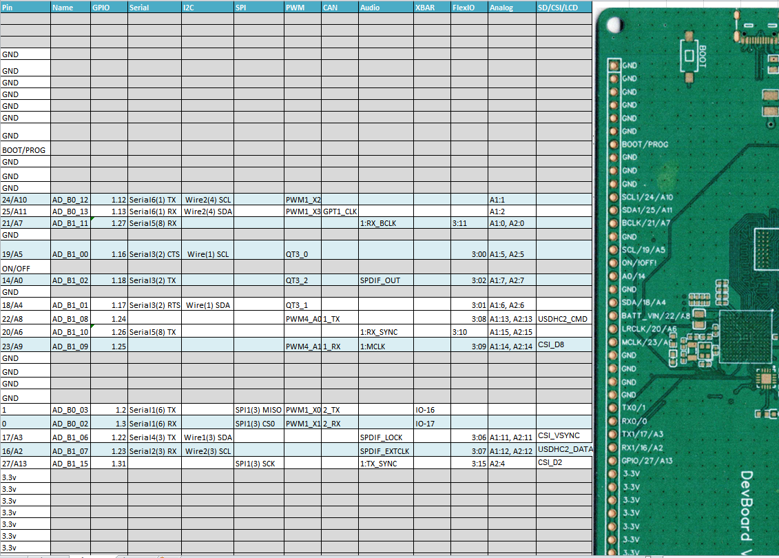
Finally got around to sitting down and mapping out all the exposed pins properly and found something odd - there's a pin labelled BATT_VIN/22/A8. My first thought: "how can this pin be both BATT_VIN and an I/O pin?" The answer is it can't/isn't; it's AD_B1_08 which is a regular IO and nothing to do with a battery. It seems on the teensy micromod this pin is connected to one-third of VIN (divided using 20K / 10K resistors).
What relevance this has to "BATT_VIN" I don't know, but I just thought I'd mention it in case anybody tried to connect a 3V coin cell to this pin and wondered why it didn't work.
What relevance this has to "BATT_VIN" I don't know, but I just thought I'd mention it in case anybody tried to connect a 3V coin cell to this pin and wondered why it didn't work.
defragster
Senior Member+
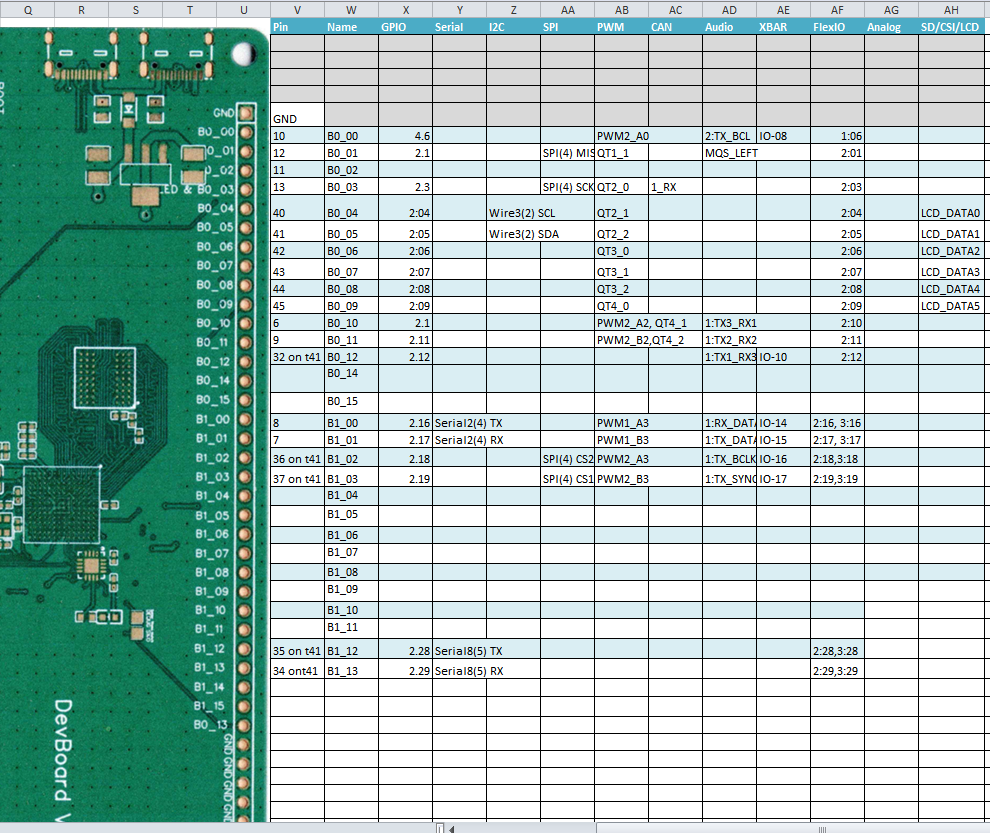
Somewhere in history back @mjs513 posted these images of the bare DevBoard I got and scanned associated with the pin names. These are in the DOCS folder of the original github by @defragster that got abandoned when the lib was forked ... not sure that XLS file with images were shared ...


What I'm wondering is why would Sparkfun connect the pin that way (on the micromod) in the first place though? Since it can't be used as a regular IO pin if it's hardwired to a constant voltage... nor can it be used in analog mode to monitor VIN (i.e. a battery level monitor) since AREF = VIN.
To be honest im not sure either. Why would you need to know supply voltage if it won't work with anything much less than 3.3v?
Also if it's battery powered there will be a DC-DC converter providing a stable 3.3v regardless of cell voltage..
Perhaps other MicroMods (such as the STM, SAMD, ESP32 etc) support something else with that specific pin
Also if it's battery powered there will be a DC-DC converter providing a stable 3.3v regardless of cell voltage..
Perhaps other MicroMods (such as the STM, SAMD, ESP32 etc) support something else with that specific pin
KurtE
Senior Member+
Not sure, but most of their carrier boards, have something like:What I'm wondering is why would Sparkfun connect the pin that way (on the micromod) in the first place though? Since it can't be used as a regular IO pin if it's hardwired to a constant voltage... nor can it be used in analog mode to monitor VIN (i.e. a battery level monitor) since AREF = VIN.
That is from their ATP board schematic. As for AREF, don't see that on their stuff. With Teensy it is probably geared more to the 3.3v pin. I don't believe raw VIN is passed to the Micromod connector.
For me the pin had issues if I wanted to use it, as for example for boards with servos, I may want to pass in lipo 3s and /3 is not large enough to get that below 3.3v
Wouldn't that be too large for VIN though? The ATP schematic says "VIN Range 2.2-6.0V".For me the pin had issues if I wanted to use it, as for example for boards with servos, I may want to pass in lipo 3s and /3 is not large enough to get that below 3.3v
If you were using your own carrier board (with a different voltage reg.), you could just use different divider resistors.
sbfreddie
Well-known member
Kurt et All:
The resistor combination you are seeing on that pin is what we in the hardware world call a "digital active termination". Why Sparkfun has done this is anybody's guess. As you have already surmised that pin will only be usable with digital circuits. There are almost no digital devices that cannot drive that active termination without any problems.
However I would not advise using it for any analog input voltages as the termination will cause large inaccuracies in any voltage applied to that pin.
Regards,
Ed
KurtE
Senior Member+
In the case of the ATP, I believe that this is due to the Voltage Regulator they choose for the board. AP7361C states:Wouldn't that be too large for VIN though? The ATP schematic says "VIN Range 2.2-6.0V".
- Wide Input Voltage Range: 2.2V – 6.0V
Looks to me like a simple voltage divider circuit.The resistor combination you are seeing on that pin is what we in the hardware world call a "digital active termination".
The only other place VIN is used, is to be fed into Voltage regulator. The actual Micromod Modules only see the 3.3v voltage. So not sure what that does to AnalogReads. Also don't see anywhere in the MicroMod pins anywhere to pass in a different Analog Reference. But could be missing something.
But as mentioned before in this thread. There is nothing with the Teensy limiting you to use this specific pin for this purpose.

