
I have mapped GPIO6 for my project this way:

So I multiplexed the high order 16-bit of GPIO6 into mix of input/output signals using latch or bi-directional buffers.
- GPIO6.PIN[32..24] = 8-bit MSB address bus as output or control/system bus as input (CLK and /WAIT in later details).
- GPIO6.PIN[23..16] = 8-bit MSB address bus as output or 8-bit data bus as input or output.
GPIO6.PIN[32..16] are connected to a set of LATCH buffers (SN74LVC573) to present an address bus as output. /AOE is connected to buffer /OE signal and ALE to buffer LE signal for address bus.
GPIO6.PIN[32..24] are also connected to a LATCH buffer (SN74LVC573) to capture control and system bus as input. ALE is connected to buffer /OE signal and 3.3V to buffer LE signal for address bus.
GPIO6.PIN[23..16] are also connected to a bi-directional buffer (SN74LVC245) to allow to present or capture data bus. /DCE is connected to buffer /CE and DDIR to buffer A->B signal (1 if T4.1 presents data bus).
I know we have :
- GPIO6_DR: bits as OUTPUT to present to physical pins. It seems it can be used to read physical pins as INPUT but a little slower than PSR?
- GPIO6_PSR: bits as INPUT to capture as seen on physical pins. What about as OUTPUT?
- GPIO6_DR_SET: fast way to set selected pins to H.
- GPIO6_DR_CLEAR: fast way to set selected pins to L.
- GPIO6_DR_TOGGLE: fast way to toggle selected pins to their opposite states.
- GPIO6_GDIR: switch individually pins to OUTPUT or INPUT mode.
What about the unused bits in GPIO6? Is it safe to set 0 or 1 to them without worrying about any conflict as long as they are not setup as GPIO?
Are also there requirements to respect to allow smooth transitions when you need latch address bus, to capture CLK and /WAIT signals, to capture data bus or present data bus without entering some conflicts?
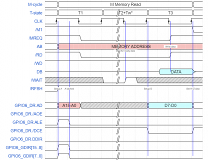
Case of Z80 memory read cycle:

Here the attempted code to do a MMRD cycle (I'm expecting the unused bit in GPIO6 are not set as GPIO pins:
So I multiplexed the high order 16-bit of GPIO6 into mix of input/output signals using latch or bi-directional buffers.
- GPIO6.PIN[32..24] = 8-bit MSB address bus as output or control/system bus as input (CLK and /WAIT in later details).
- GPIO6.PIN[23..16] = 8-bit MSB address bus as output or 8-bit data bus as input or output.
GPIO6.PIN[32..16] are connected to a set of LATCH buffers (SN74LVC573) to present an address bus as output. /AOE is connected to buffer /OE signal and ALE to buffer LE signal for address bus.
GPIO6.PIN[32..24] are also connected to a LATCH buffer (SN74LVC573) to capture control and system bus as input. ALE is connected to buffer /OE signal and 3.3V to buffer LE signal for address bus.
GPIO6.PIN[23..16] are also connected to a bi-directional buffer (SN74LVC245) to allow to present or capture data bus. /DCE is connected to buffer /CE and DDIR to buffer A->B signal (1 if T4.1 presents data bus).
I know we have :
- GPIO6_DR: bits as OUTPUT to present to physical pins. It seems it can be used to read physical pins as INPUT but a little slower than PSR?
- GPIO6_PSR: bits as INPUT to capture as seen on physical pins. What about as OUTPUT?
- GPIO6_DR_SET: fast way to set selected pins to H.
- GPIO6_DR_CLEAR: fast way to set selected pins to L.
- GPIO6_DR_TOGGLE: fast way to toggle selected pins to their opposite states.
- GPIO6_GDIR: switch individually pins to OUTPUT or INPUT mode.
What about the unused bits in GPIO6? Is it safe to set 0 or 1 to them without worrying about any conflict as long as they are not setup as GPIO?
Are also there requirements to respect to allow smooth transitions when you need latch address bus, to capture CLK and /WAIT signals, to capture data bus or present data bus without entering some conflicts?
Case of Z80 memory read cycle:
Here the attempted code to do a MMRD cycle (I'm expecting the unused bit in GPIO6 are not set as GPIO pins:
Code:
				// T1
				clk_rising_edge(); // Wait for T1 Rising Edge

				GPIO7_DR_CLEAR = nM1;
				GPIO8_DR_SET   = nRFSH;
				GPIO6_DR       = ALE | nDCE | (address << 16);
				GPIO6_DR_GDIR  = 0xFFFF0000 | nAOE | ALE | nDCE| DDIR;

				// Isn't it too short to latch bus address?

				GPIO6_DR_CLEAR = ALE; // Needs to clear ALE to capture CLK
				GPIO6_DR_GDIR  = 0x00000000 | nAOE | ALE | nDCE| DDIR;
				clk_falling_edge(); // Wait for T1 Falling Edge

				GPIO7_DR_CLEAR = nMREQ | nRD;

				// T2 / Tw
				clk_falling_edge(); // T2  Falling Edge

				while ((GPIO6_PSR & nWAIT) != nWAIT)
					clk_falling_edge(); // Tw Falling Edge

				// T3
				clk_rising_edge(); // T3 Rising Edge

				GPIO6_DR_CLEAR = nDCE; // Allow data bus capture

				clk_falling_edge(); // T3 Falling Edge

				data = uint8_t(GPIO6_PSD >> 16);

				GPIO6_DR_SET = nDCE;
				GPIO7_DR_SET = nMREQ | nRD;
Attachments
Last edited: