Weird SPI Clock Signal on Teensey 4.1, Pin 13

c172jeff

Well-known member
The PCB I designed seems to work ok when I do not connect a 1 foot connector of ribbon cable that breaks out the SPI lines as well as some other signals. When testing with the cable, the SPI seems to fail in having good communication with the 5 chips on the PCB, the cable is unconnected to anything but the PCB at this point. It does not look like I can connect more spi devices on the cable.

I am running the SPI at 1 MHz. I decided to take a look at the SPI clock to see what it might look like before and after the cable is attached. I figured at 1Mhz, it should not be a problem.

When my program is running and I scoped Pin 13, I see the below.....

Why are there 2 different frequencies on the SCK signal? It looks like a pattern at about 1Mhz and 100 Khz. I think I see this same pattern when the cable is either attached or not. In any case, what will this cause behavior? I would think that the SPI clock line should be a constant pattern/frequency if it is on and it could only be either on or off. For starters, to me this does not look proper..please advise
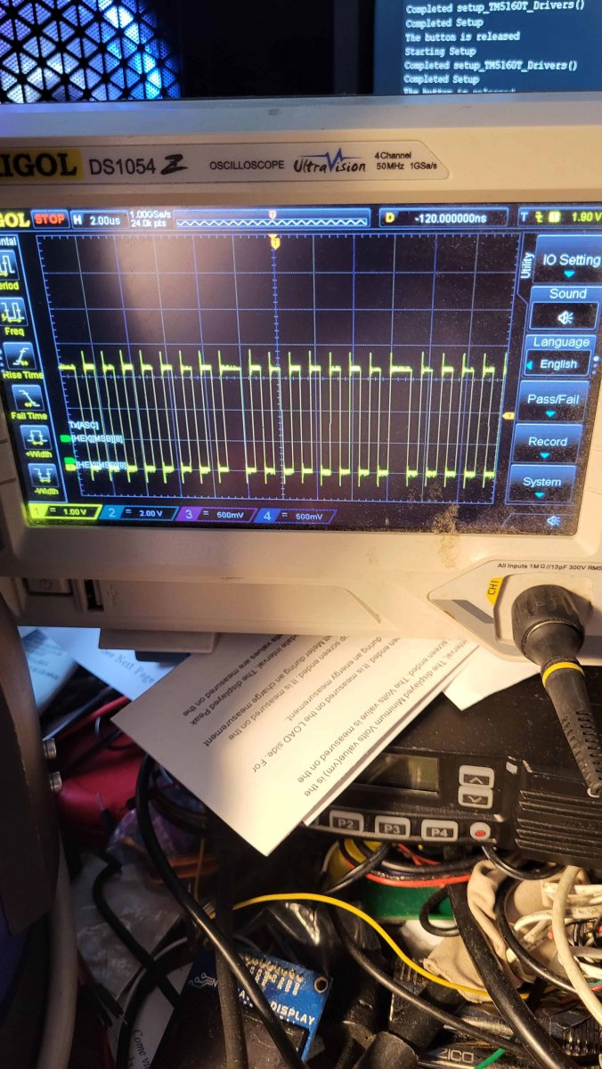


weird spi clock.jpg
 
when I do not connect a 1 foot connector of ribbon cable that breaks out the SPI lines as well as some other signals. When testing with the cable, the SPI seems to fail in having good communication with the 5 chips on the PCB, the cable is unconnected to anything but the PCB at this point.
what will this cause behavior?

The rising and falling edges of the SPI clock have very high bandwidth, even though the actual clock rate is only 1 MHz. High bandwidth signals on long cables have all sorts of difficult problems when the source impedance isn't matched to the cable's characteristic impedance. The most common solution is to place a resistor in series close to Teensy pin 13 (SCK). Same of MOSI.

To see waveforms, check out the OctoWS2811 page and scroll down to "Signal Quality".

You can find an incredible amount of information about signal quality and transmission lines online and in engineering textbooks. It's a deep rabbit hole. But in the end, for this sort of application where you have an ordinary digital signal and a "long" wire, the solution is to add a resistor approximately equal to the cable's anticipated characteristic impedance. If you don't know that spec (it's rarely given) just guess 100 to 150 ohms.

Something to keep in mind is your 50 MHz scope can't show you the very high frequency effects, but even in this photo it is showing some of the overshoot and undershoot at each rising and falling edge. If you were to use a much higher bandwidth scope, with matching high bandwidth 10X probes, and careful wiring between the cable and scope probe to minimize extra ground lead, you would see much worse overshoot and probably also very high frequency ringing. But that sort of gear is extremely expensive and difficult to set up properly, all for a solution that ends up being a cheap resistor.


Why are there 2 different frequencies on the SCK signal?

Bursts of 8 clocks is very common for SPI. The gaps between are software overhead. You can usually minimize this with SPI.transfer(buffer, size) rather than calling SPI.transfer(byte) for each individual byte.
 
Thanks Paul, this is a wealth of information. Version 2 of the board will have to have those resistors. I wonder if I could use a NanoVNA to measure the impedance perfectly and get the exact resistor in series with MOSI and SCK.
 
Paul’s comments and suggestions are spot on as for root cause and a remedy.

Another pitfall is SPI mode selection errors. Master reading MISO right when SCK toggles may still work with short wires, but fail with long.

The Teensy MCU offers many features for limiting output pin rise and fall times (bandwidth), adding schmitt trigger for inputs (the SCK pin is both output and input in SPI master mode!!) etc. The default T4 SPI library does not use those features. But it is possible to poke the IOPAD registers for the relevant pins.
 
Thanks, I am a licensed ham radio operator. Being a licensed ham radio operator, I get to scratch the surface of things electrical.

Is what Paul is talking about the concept of impedance matching... The idea of matching transmitter to feed line to antennae/load?
In ham radio, if this is not done, you can get damaging reflections and I suppose what looks like ringing on an oscilloscope.

In ham radio, you can always force a match by using an antenna tuner. This is usually a combination of L, C, and R at the source. Once done, and matched, I suppose no more ringing/standing waves.

If this is what's happening here, and I suppose it is, I probably should always make PCB's with the provision I can add a shunt to ground as well as some L and C on SCK and MISO (if need be)? If they are not needed, I can just short them to look the same as a single trace.

Anyways, in ham radio, I can use a NanoVNA to do all sorts of neat things...most are above my pay grade.

Can I use a NanoVNA on my PCB with a Teensey to measure the velocity factor of the trace and SWR to perfectly add something to match SCK and MOSI?


If I perfectly match the impedance of the source (Teensey) against the transmission line (the trace and what follows)..., will this ringing completely disappear?

It works as is....just not with the longer cable attached.

I wonder about adding an arbitrary cable length in the future and matching it ->no ringing -> no problems ... Wondering if this an over simplification and more importantly, what are the main points I am missing. I like the idea of matching impedances, and am curious if an "antenna tuner" on my PCB would completely eliminate ringing?
 
Yes, Z matching is part of the solution.
Source output Z on the Teensy side can be tweaked by either a series R as Paul suggested, but you can also opt for using the drive strength, slew rate and speed settings in the iMXRT1062 chip for the SCK output pin. Finding the relevant IOMUXC_SW_PAD_CTL_PAD_GPIOxxyy registers is a bit of a pain because T4 has 3 SPI hardware ports defined, numerated in Arduino land as 0, 1, 2, but for NXP known as LPSPI4, LPSPI3, LPSPI1 or so, and then SPI pins rerouted via MUXSELs to end up on PORT pins numbered inconsistently in Arduino land. But it's doable. I think the default T4 first SPI port SPC pin is "pin 13" which is on GPIO_B0_03. So IOMUXC_SW_PAD_CTL_PAD_GPIO_B0_03 is the register to tweak. I think...

Still it's all a bit more subtle as just tweaking pin output impedance at the signal source and then assuming all will be fine. At the other end of the wire where the (last) SPI slave sits, there's another unterminated transmission line, open ended, so there things (sharp edges) still bounce back. And thus possibly causing spurious edges on the T4 SPC output pin. Which you thought was a (strong) output only, but actually it is also the input to the T4 SPI shift registers. False edges there, enough amplitude, Schmitt trigger (HYST) disabled, do make the T4 LPSPI SPI shift register decide to shift - prematurely...

Besides Z (mis)matching, basic capacitive loading of the SCK pin can bite you (or hide eminent problems). Too much capacitance on SCK and no HYST enabled makes you vulnerable...

How good or bad the SPI slave chip is (Schmitt trigger on SCK yes/no, bandwidth limiting filters in its SCK input etc) also matters.
And decent ground planes are a must...
 
Last edited:
On my board, I am noting that if I do not connect the Oscilloscope, the Board mostly works (95% of the time).
By that I mean, SPI messages get sent to/from the various devices.

Connecting the Oscilloscope, which has short connections, seems to damage the SPI signal to a point that this good communication breaks.
Nothing is accurately sent to/from the various SPI devices when the O scope is connected. The SPI devices are all on the same 80mm square board.

So, I looked into IOMUXC_SW_PAD_CTL_PAD_GPIO_B0_03 to see its effect on Pin 13, SCK.

After my SPI.begin() call, I

ran code such as

IOMUXC_SW_PAD_CTL_PAD_GPIO_B0_03 &= ~IOMUXC_PAD_SRE;


to change the slew rate to slow. It seems to do nothing at all. I am looking at the ringing on my O-scope and would have expected a change when either switching the bit on or off. I do not see any change. I am sure that IOMUXC_SW_PAD_CTL_PAD_GPIO_B0_03 is the proper link as when I set DSE to 0, my output signal disappears from the O scope.

I had seen this post,
https://forum.pjrc.com/index.php?threads/slew-rate-limiting-for-spi.71455/ and noted that that person saw the same thing - IOMUXC_PAD_SRE has no effect

I saw something about user space and wonder if the microprocessor on the Teensey is running in that space and if that prevents these types of changes?...

Does anyone know how to use the macros shown in
IOMUXC_SW_PAD_CTL_PAD_GPIO_B0_03 |= IOMUXC_PAD_SPEED(1) | IOMUXC_PAD_DSE(4) | IOMUXC_PAD_SRE;

to make changes to the slew rate on Pin 13 or more importantly, if it is achievable in a line of code right after SPI.begin().


I am hoping to change the slew rate to slow and/or the drive strength and see effects on my 100Mhz scope.
 
Can I use a NanoVNA on my PCB with a Teensey to measure the velocity factor of the trace and SWR to perfectly add something to match SCK and MOSI?

I'm not very familiar with this measurement, but I'm going to go out on a limb to answer "probably not". A network of PCB traces, and separate ground return paths if not a 4+ layer PCB with unbroken ground plane, coupled to a completely different cable probably having PVC plastic rather than FR4 fiberglass for dialectric, and 5 destination points that are mostly capacitive loads (but could be quite non-linear... think MOSFET gate & diode junctions rather than real capacitor with pure insulator dialectric) is likely quite a bit more complex than the intended application. I'm a bit skeptical you'd end up with a useful measurement.

But typically just getting the resistor value "close" (even within 30-50% of "ideal") makes a huge improvement. Often the resistor forming a slight low-pass filter together with the capacitance of the traces and nearby chip pins (typically 5pF per pin) has as much or more effect than the source impedance matching to characteristic impedance of the wiring.

I saw something about user space and wonder if the microprocessor on the Teensey is running in that space and if that prevents these types of changes?...

This question is much easier to answer. By default all code runs in system mode with full access to all hardware registers. You can reconfigure the pin and GPIO registers.

While unrelated to hardware registers, for a complete answer (especially for people who later find this by search), on Teensy 4.x we do configure the MPU (memory protection unit) to restrict executing instructions from memory normally used for data, and from writing to memory normally used for executing instructions. This is meant as a proactive software security measure, to prevent many types of programming errors from becoming potentially exploitable for code execution. The MPU also disallows any access to the first 32 bytes of memory, intended to catch NULL pointer dereference errors. For peripheral registers, the default MPU setting allows full access.
 
Last edited:
c172jeff, what are the SPI slaves that you use? If these are the ST MEMS (magnetometers, gyro, accelerometers etc) then there are lots of pitfalls with I2C interface mode getting activated by accident. And issues with SDO lines being undefined when first SCK clock edge arrives. Maybe that’s what’s biting you?
The scope probe is 1x or 10x? A small capacitor (~22 pF ish) has the same effect as adding the scope probe?
 
Those SPI slaves claim to have 20ns filters on their SCK inputs to avoid false triggering. So that should be pretty tolerant to ringing with the wire lengths that you have. The T4 SPI clock input may however still be suffering…
Things to double check also:
* Is SPI MODE3 the mode that T4 uses?
* Is tCC always respected?
* Is tCH always respected?
* Edges in SDI or SDO within +/- 100 ns of SCK rising?

SPI communication errors could be:
* failure of delivering data to slave
* failure of capturing data from the slave

I would try to diagnose what really goes wrong by exploiting the loopback after 40 bits feature that the TMC5160 offers: keep CS low, let Teensy send random bit stream and check that exactly the same data gets echoed 5 bytes later. If not then drive a leftover T4 output high, trigger your scope on that, and see who’s to blame for misbehaving.

IMG_0556.png
 
You define which SPI mode when you use the bus. Wouldn't expect any timing problems so long as respect the max freq.
 
I am using a Mode 3 SPI bus. I verified that in the oscilloscope and see it defined in code.

By the way, here is a short video of the board in a "working state"


If you connect the O scope, it no longer works as in the video. Same with the Raspberry pi. Connect the Pi and improper SPI communication ensues.

I do think that some parts of the SPI data stream are lost or miscommunicated.

When I designed the board, I laid the traces for the SPI signals without any regard for being proper. I mean they take twists and turns to get to the various places. One of them might even be a 165 degree turn around a pin and through vias. It is a 4 layer board. Next board will be different. I really had no idea I would have SPI issues.

I saw that SPI reference page in the manual and will have to study that next with regard to timings. I run the communication at 1M. It is not exactly a 1M SPI clock, more like 9xx Khz.

I had no idea that I could "to diagnose what really goes wrong by exploiting the loopback after 40 bits feature that the TMC5160 offers: keep CS low, let Teensy send random bit stream and check that exactly the same data gets echoed 5 bytes later." That looks like the feature to work with next to debug this problem." I will definitely use that to find the real culprit.


Earlier, when I decoded the SPI signals on the Oscilloscope, for the most part the values sent were correct. At times though, when I though a value should show on the O scope, it was 0, so not 100%.

I am really surprised I got this far on my first real test of SPI on a PCB.
 
is your 'scope probe set to x10? It needs to be for most situations so it has minimal loading on the circuit and full bandwidth.
 
Yes, I have been using 10x. I am looking at the timings/traces on my oscilloscope. I think i see a problem.
I am triggering on a falling edge of the chip select line. Most timings/triggers look as expected. Clock is high before cs falls (as per the doc).
I just noticed a pulse of this line in between clock edges. Blue is Chip Select. Yellow is the clock.
I cannot think of a situation where this should be true. I need to look more into this and the TM5160 library.
I plan to get the eval board for the tm5160 and link that to my motors to experiment and have a look at ideal signals.
Also the loop back test I plan to do. First, I want to understand where this pulse is coming from and why? I think the clock should always be high before this falls. This might be the issue. I used a TM5160 library from github.


20240108_112459.jpg
 
Back
Top